Method for manufacturing gate oxide layer of EEPROM and gate oxide layer manufactured thereby

A technology of gate oxide layer and manufacturing method, which is applied in semiconductor/solid-state device manufacturing, electrical components, electrical solid-state devices, etc., can solve the problems of long time required, many process steps, high manufacturing cost, etc., speed up the speed and reduce the manufacturing cost Effect of reducing cost and manufacturing time

Active Publication Date: 2011-06-22
SHANGHAI HUAHONG GRACE SEMICON MFG CORP
View PDF4 Cites 11 Cited by
  • Summary
  • Abstract
  • Description
  • Claims
  • Application Information

AI Technical Summary

Problems solved by technology

[0015] The existing method for manufacturing the gate oxide layer of EEPROM requires two thermal oxidation growth processes plus one photolithography and etching proce

Method used


Image

  • Method for manufacturing gate oxide layer of EEPROM and gate oxide layer manufactured thereby
  • Method for manufacturing gate oxide layer of EEPROM and gate oxide layer manufactured thereby
  • Method for manufacturing gate oxide layer of EEPROM and gate oxide layer manufactured thereby

Examples


Embodiment Construction

[0030] The manufacture method of the gate oxide layer of EEPROM of the present invention comprises the steps:

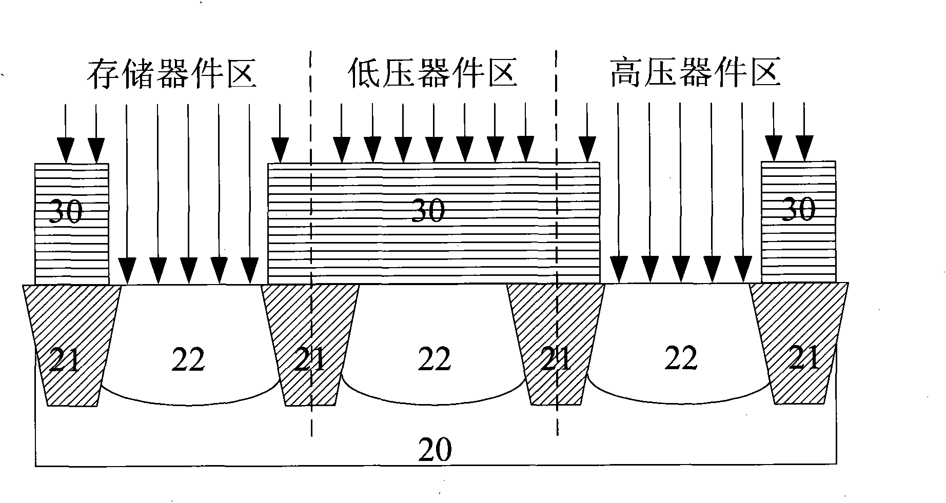
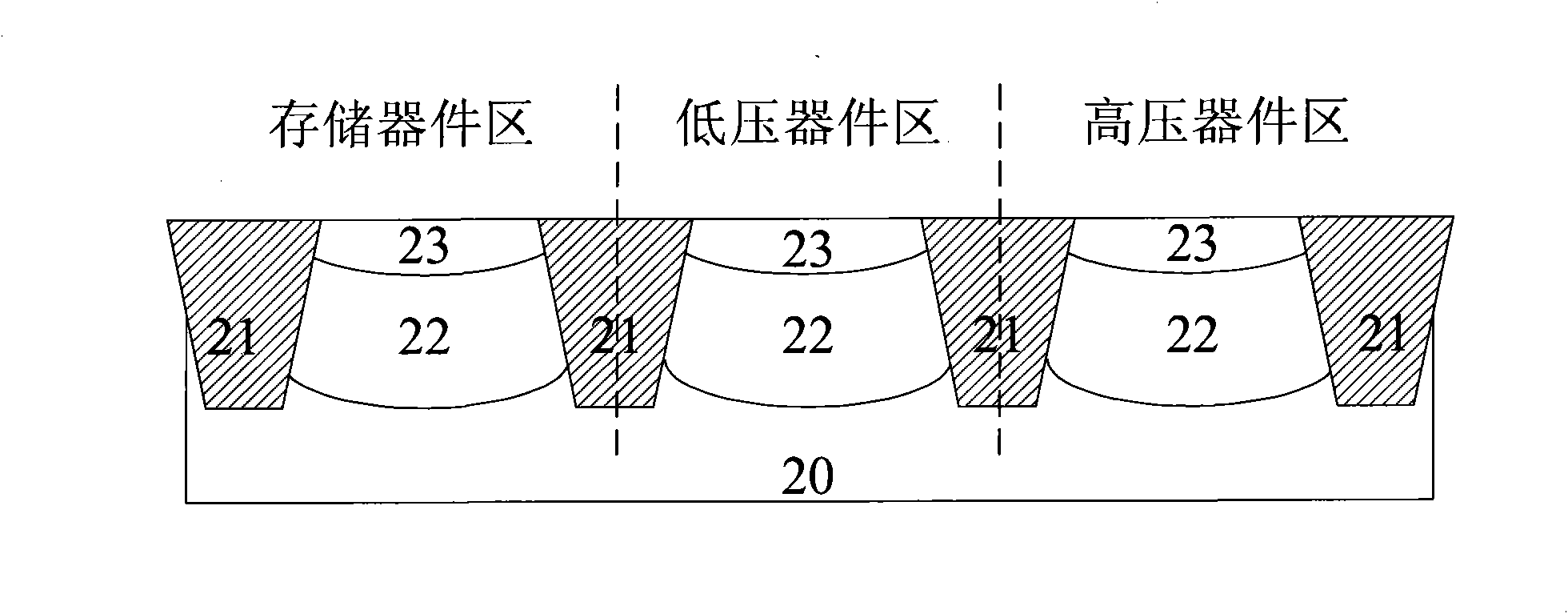
[0031] The initial state of the silicon wafer is: an isolation region 21 has been formed in the silicon substrate 20 by a field oxygen isolation (LOCOS) or shallow trench isolation (STI) process, and a p-well 22 is also formed in the silicon substrate 20 by an ion implantation process, Multiple p-wells 22 are isolated by multiple isolation regions 21 .

[0032] Step 1, see Figure 3a Spin-coat a layer of photoresist 30 on the surface of the silicon wafer. After exposure and development, the photoresist 30 only covers the low-voltage device region and the region where the tunnel oxide layer will be formed. In the storage device region, the region other than the tunnel oxide layer is exposed. , the high-voltage device area is fully exposed. Ion (atom) implantation is performed on the surface of the silicon wafer, and the photoresist 30 serves as a barrier layer for i...


PUM


Abstract

The present invention discloses a method for manufacturing a gate oxide layer of an EEPROM (Electrically-Erasable Programmable Read-Only Memory). The method comprises the following steps: step 1, spin-coating a layer of photoresist on the surface of a silicon chip, wherein after exposing and developing, the photoresist only covers a low voltage device area and an area on which a tunneling oxide layer will form, wherein a storage device area is fully exposed except the area containing the tunneling oxide and a high pressure device area is also fully exposed; carrying out an ion implantation onthe surface of the silicon chip with the photoresist as a barrier layer of the iron implantation; and forming an ion implantation area in the silicon chip; step 2, removing the photoresist; step 3, making a high voltage oxide layer and a tunneling oxide layer grow on the surface of the silicon chip; and making a high pressure oxide layer grow in the ion implantation area formed in the step 1, wherein the thickness of the tunneling oxide layer is less than the thickness of the high voltage oxide layer. The present invention also discloses a gate oxide layer of an EEPROM manufactured by the above method. The method for manufacturing a gate oxide layer of an EEPROM has the advantages of simple processing steps, short manufacture time and low manufacture cost. Moreover, electrical characteristics of a low voltage device area can be improved.

Description

technical field [0001] The invention relates to a manufacturing method of EEPROM (Electrically-Erasable Programmable Read-Only Memory, Electrically Erasable Programmable Read-Only Memory). Background technique [0002] see figure 1 , The existing EEPROM memory cell is composed of a selection transistor 1a and a floating gate transistor 1b. Wherein, the selection transistor 1a is usually an NMOS, and performs a gate function; the floating gate transistor 1b is usually an n-channel MOS transistor, and performs a data storage function. The selection transistor 1a and the floating gate transistor 1b share a source and drain region 11 . The floating gate transistor 1b comprises two gates 13a, 13b, with the floating gate 13a below and the control gate 13b above. [0003] In addition to the storage unit of the EEPROM, there are peripheral devices, and the peripheral devices include low-voltage devices and high-voltage devices. Typical peripheral low-voltage devices such as IO (...

Claims


Application Information

Patent Timeline
IPC IPC(8): H01L21/8247H01L21/28H01L27/115
Inventor 张可钢陈昊瑜
Owner SHANGHAI HUAHONG GRACE SEMICON MFG CORP
Why Eureka
Try Eureka