Flexible substrate and preparation method thereof
A flexible substrate, plastic-based technology, applied in semiconductor/solid-state device manufacturing, electrical components, electric solid-state devices, etc., can solve the problems of increasing the preparation cycle of FOLED substrates, expensive thin-film packaging equipment, and increasing the cost of processing substrates. Production time period, strong water absorption, and the effect of reducing production cost
- Summary
- Abstract
- Description
- Claims
- Application Information
AI Technical Summary
Problems solved by technology
Method used
Image


Examples
Embodiment 1
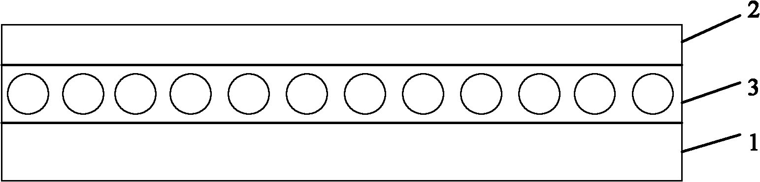
[0027] The flexible substrate for FOLED includes an organic polymer plastic substrate, an ITO semiconductor transparent conductive film, and a molecular sieve film layer coated between them. The manufacturing method of the flexible substrate is: firstly, the molecular sieve film layer is coated on the organic polymer plastic substrate. , and then coat the ITO semiconductor transparent conductive film on the molecular sieve film layer to obtain a flexible substrate.
[0028] The flexible substrate for FOLED as shown in the accompanying drawings includes an ITO semiconductor transparent conductive film 2 with a thickness of 0.2 μm, a molecular sieve film layer 3 with a thickness of 10 μm in the middle layer, and an organic polymer PET plastic substrate with a thickness of 50 μm (hereinafter referred to as the substrate) 1. Molecular sieve film layer 3 is prepared by uniformly dispersing molecular sieve particles in a polymer adhesive. The polymer adhesive in this example is an ul...
Embodiment 2
[0035]The difference between the flexible substrate for FOLED and the first embodiment is that the thickness of the molecular sieve film layer 3 is 20 μm.
[0036] The fabrication steps of the flexible substrate are as follows:
[0037] 1) Preparation of molecular sieve film layer 3: same as Step 1) of Example 1.
[0038] 2) Coating the molecular sieve film layer 3: the difference from step 2) in the first embodiment is that the rotation speed of the spin coating equipment is set to 600 RPM, and the thickness of the molecular sieve film layer 3 obtained by coating is 20 μm.
[0039] 3) Deposition of the ITO semiconductor transparent conductive film 2: the same as step 3) of the first embodiment.
[0040] The water vapor permeability of the flexible substrate obtained in this embodiment is measured by a measurement system for the permeability of organic optoelectronic device packaging materials to be 1.63×10 -6 g / m 2 d, The water vapor permeability of the organic polymer PET...
PUM
| Property | Measurement | Unit |
|---|---|---|
| Thickness | aaaaa | aaaaa |
| Thickness | aaaaa | aaaaa |
| Thickness | aaaaa | aaaaa |
Abstract
Description
Claims
Application Information
 - R&D Engineer
- R&D Manager
- IP Professional
- Industry Leading Data Capabilities
- Powerful AI technology
- Patent DNA Extraction
Browse by: Latest US Patents, China's latest patents, Technical Efficacy Thesaurus, Application Domain, Technology Topic.
© 2024 PatSnap. All rights reserved.Legal|Privacy policy|Modern Slavery Act Transparency Statement|Sitemap