Groove-shaped channel AlGaN/GaN-reinforced high electron mobility transistor (HEMT) component and manufacturing method thereof

An enhanced, channel technology, applied in the field of microelectronics, can solve the problems of inability to meet the threshold voltage requirements of switching applications, the influence of device performance and reliability, and the low threshold voltage, to eliminate polarization effects and achieve good anisotropy. , the effect of improving electrical characteristics and threshold voltage

Inactive Publication Date: 2011-07-20
XIDIAN UNIV
View PDF5 Cites 40 Cited by
  • Summary
  • Abstract
  • Description
  • Claims
  • Application Information

AI Technical Summary

Problems solved by technology

[0006] In 2000, Hu et al. used the selective regrowth PN junction gate technology to successfully develop an enhanced mode AlGaN/GaN HEMT device, but its peak transconductance was only 10mS/mm
These technologies still have great shortcomings: first, the threshold voltage is not high, and the highest reported is only 0.9V, which cannot meet the threshold voltage requirements of switching applications; second, whether etching to form grooves or fl

Method used


Image

  • Groove-shaped channel AlGaN/GaN-reinforced high electron mobility transistor (HEMT) component and manufacturing method thereof
  • Groove-shaped channel AlGaN/GaN-reinforced high electron mobility transistor (HEMT) component and manufacturing method thereof
  • Groove-shaped channel AlGaN/GaN-reinforced high electron mobility transistor (HEMT) component and manufacturing method thereof

Examples


Embodiment 1

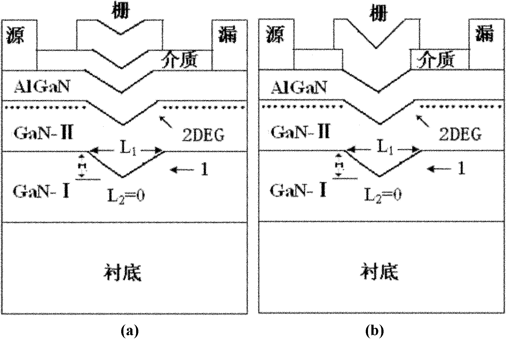
[0058] refer to figure 1 (a), the AlGaN / GaN enhanced MIS gate HEMT device of the present invention, the structure from top to bottom is: substrate, I-GaN layer, II-GaN layer, AlGaN barrier layer, source level, drain electrode, dielectric layer and the gate, wherein the two ends of the barrier layer are the source and the drain, and the middle of the I-GaN layer is provided with a triangular groove (1), the depth of the groove: H is 100-600 nanometers, which is less than the thickness of I-GaN , the length of the upper base of the groove is L 1 , the value ranges from 0.1 to 0.5 microns, and the length of the lower bottom is L 2 = 0, two-dimensional electron gas 2DEG is formed on the plane interface of II-GaN and AlGaN, and the concentration of 2DEG is very low or almost non-existent on the inclined interface of II-GaN and AlGaN, and the dielectric layer is located on the upper part of the source and drain and the upper part of the barrier layer between the source and the dra...

Embodiment 2

[0060] refer to figure 1 (b), the AlGaN / GaN enhanced MS gate HEMT device of the present invention, the structure is from top to bottom: substrate, I-GaN layer, II-GaN layer, AlGaN barrier layer, source, drain, dielectric Layer and gate, wherein the two ends of the barrier layer are source and drain, and a triangular groove (1) is arranged in the middle of the I-GaN layer. The depth of the groove: H is 100-600 nanometers, which is less than the thickness of I-GaN , the length of the upper base of the groove is L 1 , the value ranges from 0.1 to 0.5 microns, and the length of the lower bottom is L 2 = 0, two-dimensional electron gas 2DEG is formed on the plane interface of II-GaN and AlGaN, and the concentration of 2DEG is very low or almost non-existent on the inclined interface of II-GaN and AlGaN, and the dielectric layer is located between the source and the drain The upper part of the potential barrier layer, the gate is located between the upper part of the potential bar...

Embodiment 3

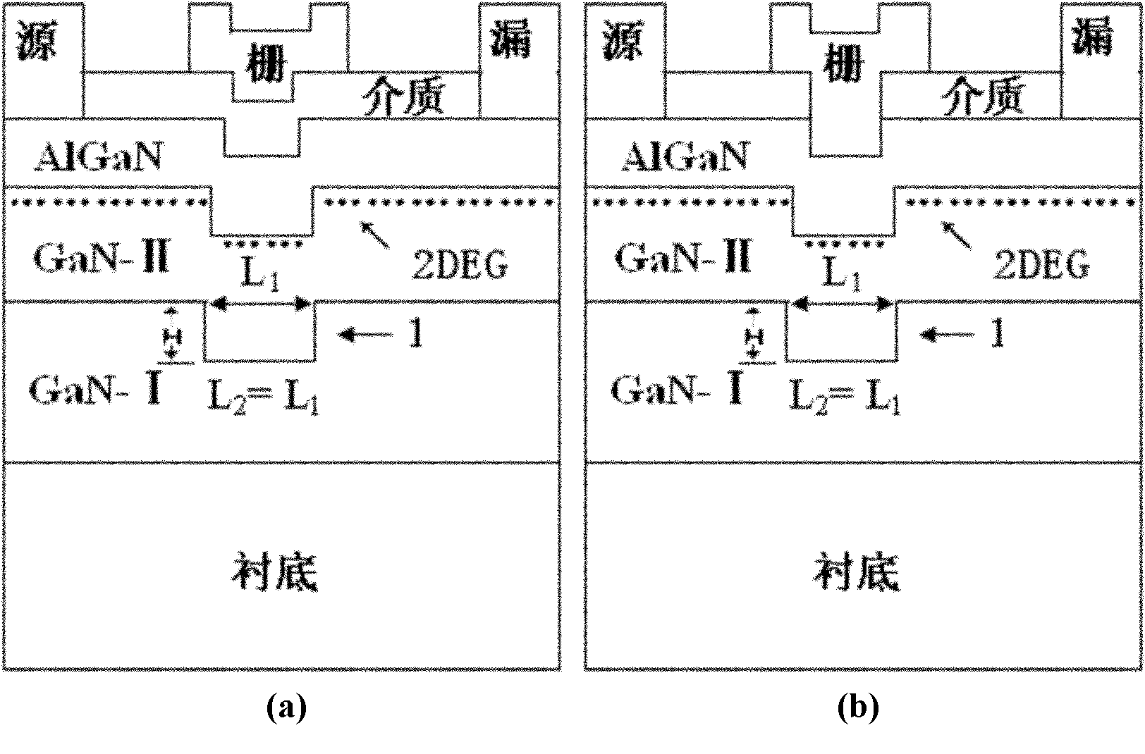
[0062] refer to figure 2 (a), AlGaN / GaN enhanced MIS gate HEMT device, the structure from top to bottom is: substrate, I-GaN layer, II-GaN layer, AlGaN barrier layer, source, drain, dielectric layer and gate The two ends of the barrier layer are the source and the drain, and a rectangular groove (1) is arranged in the middle of the I-GaN layer. The depth of the groove: H is 100-600 nanometers, which is less than the thickness of the I-GaN. The length of the upper base is L 1 , the value ranges from 0.1 to 0.5 microns, and the length of the lower bottom is L 2 =L 1 , a two-dimensional electron gas 2DEG is formed on the plane interface of II-GaN and AlGaN, and the concentration of 2DEG is very low or almost non-existent on the vertical interface of II-GaN and AlGaN, and the dielectric layer is located on the upper part of the source and drain and the source The upper part of the barrier layer between the electrode and the drain, and the gate is located on the upper part of t...


PUM

PropertyMeasurementUnit
Thicknessaaaaaaaaaa
Thicknessaaaaaaaaaa
Thicknessaaaaaaaaaa

Abstract

The invention discloses a groove-shaped channel AlGaN/GaN-reinforced high electron mobility transistor (HEMT) component and a manufacturing method thereof and mainly solves the problem of low reliability caused by a low threshold voltage of the conventional reinforced component and large etching damage in the manufacturing process. The component comprises a substrate, an I-GaN layer, a II-GaN layer, an AlGaN barrier layer, a source, a drain, a medium layer and a grid from the bottom up, wherein a groove (1) is formed in the middle of the I-GaN layer so as to form a two-dimensional electronic gas (2DEG) on the planar interface between the II-GaN and the AlGaN, while the 2DEG cannot be formed on an inclining interface between the II-GaN and the AlGaN. According to different processes, the reinforced component structure can be manufactured into two types of components, namely a metal oxide semiconductor grid and a Schottky grid. The invention has the advantages of high reliability, simple process and good repeatability and can be used in high-temperature, high-frequency and large-power places, large-power switches and digital circuits.

Description

technical field [0001] The invention belongs to the technical field of microelectronics and relates to semiconductor materials and device manufacturing techniques, in particular to a novel AlGaN / GaN enhanced HEMT device structure and manufacturing method, which can be used in high-temperature and high-power applications and constitute digital circuit basic units. Background technique [0002] With the development of modern weaponry and aerospace, nuclear energy, and communication technologies, higher requirements are placed on the performance of semiconductor devices. As a typical representative of wide bandgap semiconductor materials, GaN-based materials have the characteristics of large bandgap width, high electron saturation drift velocity, high breakdown field strength and good thermal conductivity, and can be used to make high-temperature, high-frequency and high-power electronic devices. More importantly, GaN-based materials can form modulation-doped AlGaN / GaN heterost...

Claims


Application Information

Patent Timeline
IPC IPC(8): H01L29/778H01L29/06H01L21/335H01L21/285
CPCH01L29/7786H01L29/7789H01L29/4236H01L29/2003
Inventor 张进成陈珂郝跃马晓华王冲付小凡马俊彩刘子扬林志宇张凯
Owner XIDIAN UNIV
Why Eureka
Try Eureka