Preparation method of multilayer transparent conductive thin film as well as prepared thin film and application thereof
A technology of transparent conductive film and powder, applied in coating, metal material coating process, vacuum evaporation coating and other directions, can solve the problems of difficult to control thickness, difficult to obtain, poor light transmittance, etc. The effect of low temperature and high stability
- Summary
- Abstract
- Description
- Claims
- Application Information
AI Technical Summary
Problems solved by technology
Method used
Image

Examples
preparation example Construction
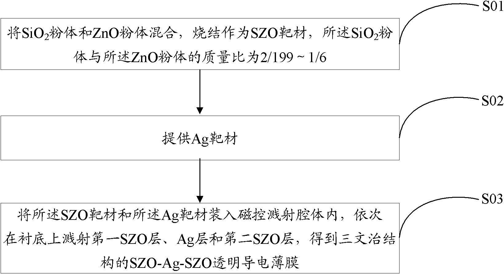
[0017] see figure 1 , showing a method for preparing a multilayer transparent conductive film according to an embodiment of the present invention, which includes the following steps:
[0018] S01: SiO 2 Powder and ZnO powder are mixed and sintered as SZO target material, the SiO 2 The mass ratio of the powder to the ZnO powder is 2 / 199-1 / 6;
[0019] S02: Provide Ag targets;
[0020] S03: Put the SZO target and the Ag target into the magnetron sputtering chamber, sputter the first SZO layer, the Ag layer and the second SZO layer on the substrate in sequence to obtain the SZO-Ag with a sandwich structure -SZO transparent conductive film.
[0021] In step S01, the SiO 2 Mix the powder and ZnO powder evenly, and sinter, for example, at a temperature of 900° C. to 1350° C. to obtain an SZO ceramic target. Preferably, SiO 2 The mass ratio of powder to ZnO powder is 1 / 70~1 / 20, more preferably, SiO 2 The mass ratio of the powder to the ZnO powder is 1 / 50˜1 / 30. In a preferred ...
Embodiment 1
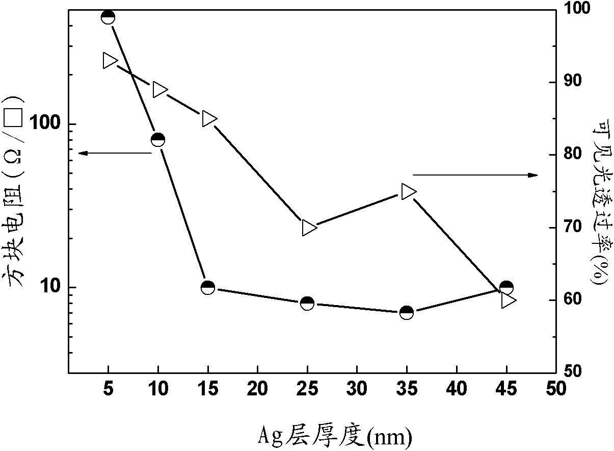
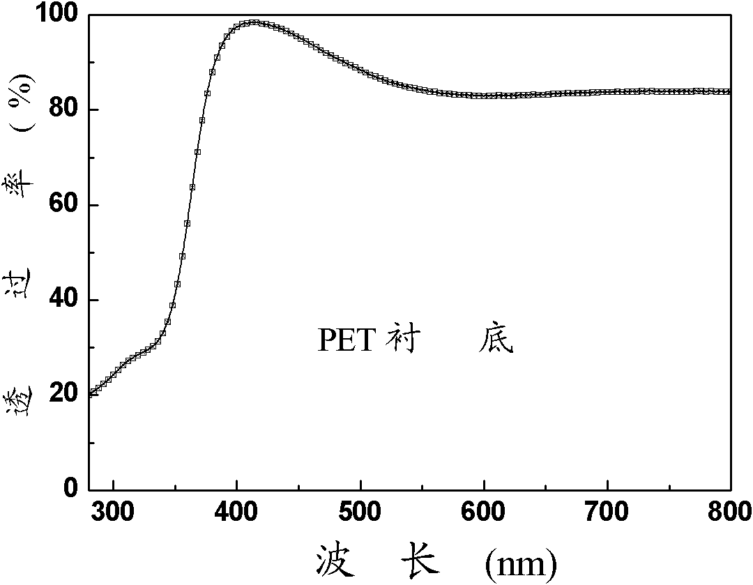
[0029] Choose SiO2 2 :ZnO=1:49 (mass ratio) powder, after being evenly mixed, sintered at 1250°C at high temperature to form a Φ60×2mm ceramic target, and put it into a vacuum chamber together with an Ag target (Φ50×3mm). Then, the PET substrate was ultrasonically cleaned with absolute ethanol and deionized water, dried with high-purity nitrogen, and placed in a vacuum chamber. The distance between the target and the substrate was set to 50mm. Use a mechanical pump and a molecular pump to evacuate the cavity to 6.0×10 -4 Pa, the argon gas of 20 sccm is introduced, and the pressure is adjusted to 1.0 Pa. The sputtering power of the first SZO layer was 20W, the sputtering power of the Ag target was 60W, and the sputtering power of the second SZO layer was 100W. The thickness of the three layers of the obtained SZO-Ag-SZO thin film is 60nm, 15nm, 60nm respectively, the sheet resistance is 8Ω / □, and the average transmittance of visible light is 90%.
Embodiment 2
[0031] Choose SiO2 2:ZnO=1:49 (mass ratio) powder, after being evenly mixed, sintered at 1250°C at high temperature to form a Φ60×2mm ceramic target, and put it into a vacuum chamber together with an Ag target (Φ50×3mm). Then, the PET substrate was ultrasonically cleaned with absolute ethanol and deionized water, dried with high-purity nitrogen, and placed in a vacuum chamber. The distance between the target and the substrate was set to 50mm. Use a mechanical pump and a molecular pump to evacuate the cavity to 6.0×10 -4 Pa, the argon gas of 20 sccm is introduced, and the pressure is adjusted to 1.0 Pa. The sputtering power of the first SZO layer was 20W, the sputtering power of the Ag target was 60W, and the sputtering power of the second SZO layer was 100W. The thickness of the three layers of the obtained SZO-Ag-SZO thin film is 75nm, 5nm, 75nm respectively, the sheet resistance is 450Ω / □, and the average transmittance of visible light is 93%.
PUM
| Property | Measurement | Unit |
|---|---|---|
| thickness | aaaaa | aaaaa |
| thickness | aaaaa | aaaaa |
| thickness | aaaaa | aaaaa |
Abstract
Description
Claims
Application Information
 - R&D
- Intellectual Property
- Life Sciences
- Materials
- Tech Scout
- Unparalleled Data Quality
- Higher Quality Content
- 60% Fewer Hallucinations
Browse by: Latest US Patents, China's latest patents, Technical Efficacy Thesaurus, Application Domain, Technology Topic, Popular Technical Reports.
© 2025 PatSnap. All rights reserved.Legal|Privacy policy|Modern Slavery Act Transparency Statement|Sitemap|About US| Contact US: help@patsnap.com