Preparation method for wide-side 808nm divided mode semiconductor laser structure

A technology of semiconductors and lasers, which is applied in the field of preparation of discrete-mode semiconductor laser structures, and can solve problems such as complex manufacturing processes, poor stability, and high sensitivity of collimated beams

Inactive Publication Date: 2011-08-10
INST OF SEMICONDUCTORS - CHINESE ACAD OF SCI
View PDF0 Cites 5 Cited by
  • Summary
  • Abstract
  • Description
  • Claims
  • Application Information

AI Technical Summary

Problems solved by technology

[0003] At present, the conventional methods for achieving single-mode wavelength stability include DFB, DBR, VCSEL, and external cavity feedback. The wavelength of the laser is highly sensitive to the epitaxial growth thickness, and the method of using the optical feedback of an external grating to achieve wavelength locking is highly sensitive to the collimated beam and has poor stability

Method used


Image

  • Preparation method for wide-side 808nm divided mode semiconductor laser structure
  • Preparation method for wide-side 808nm divided mode semiconductor laser structure
  • Preparation method for wide-side 808nm divided mode semiconductor laser structure

Examples


preparation example Construction

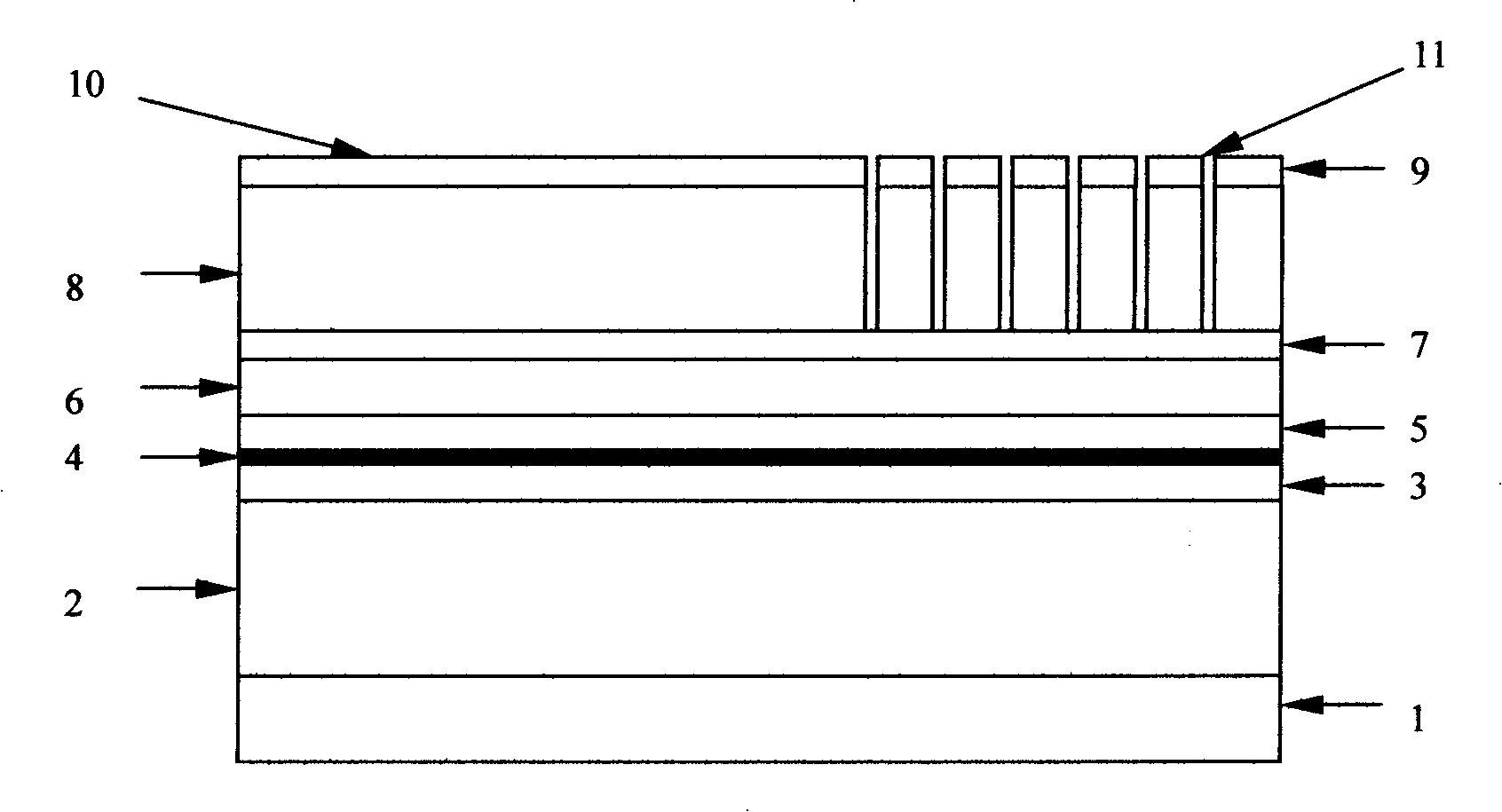
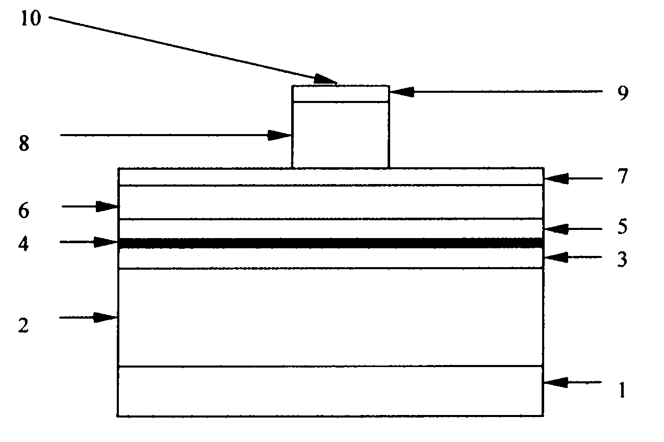
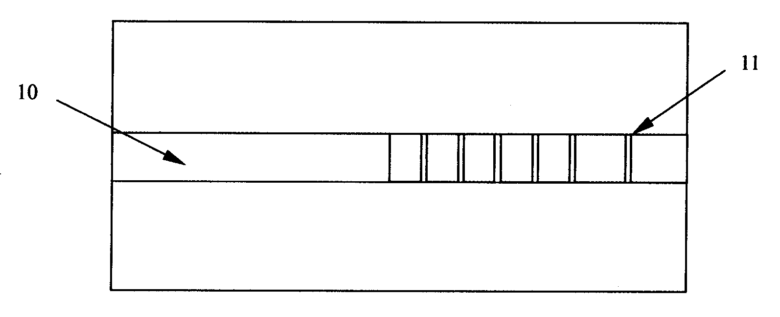
[0025] see figure 1 , figure 2 and image 3 , the invention provides a kind of preparation method of wide-face 808nm discrete mode semiconductor laser, comprises the steps:

[0026] Step 1: Take a GaAs substrate 1;

[0027] Step 2: Prepare N-type AlGaAs lower confinement layer 2, lower waveguide layer 3, quantum well layer 4, upper waveguide layer 5, first P-type upper confinement layer 6, etch cut-off layer on GaAs substrate 1 in sequence 7. The second P-type upper confinement layer 8 and P-type cap layer 9; wherein the lower confinement layer 2 is a highly doped N-type aluminum gallium arsenic material (Al 0.53-0.55 Ga 0.45-0.47 As), the Si doping concentration is 1×10 18 cm -3 , with a thickness of 1.5 μm, the purpose is to limit the diffusion of carriers in the active region, so as to reduce the threshold current and improve efficiency; the lower waveguide layer 3 is made of non-doped aluminum gallium arsenic material (Al 0.33-0.35 Ga 0.65-0.67 As) with a thicknes...

Embodiment

[0031] see again figure 1 , figure 2 and image 3 Shown, the present invention the present invention provides a kind of preparation method of wide-face 808nm discrete mode semiconductor laser, comprises the steps:

[0032] Step 1: Take a GaAs substrate 1;

[0033] Step 2: Prepare N-type AlGaAs lower confinement layer 2, lower waveguide layer 3, quantum well layer 4, upper waveguide layer 5, first P-type upper confinement layer 6, etch cut-off layer on GaAs substrate 1 in sequence 7. The second P-type upper confinement layer 8 and P-type cap layer 9; wherein the lower waveguide layer 3 is made of undoped AlGaAs material, wherein the quantum well layer 4 is made of undoped AlGaInAs material, wherein the upper The waveguide layer 5 is made of non-doped AlGaAs material, wherein the first P-type upper confinement layer 6 is made of highly doped AlGaAs material with a thickness of 0.2 μm, and the etching cut-off layer 7 is highly doped P-type Indium gallium phosphide material w...


PUM


Abstract

The utility model provides a preparation method for a wide-side 808nm divided mode semiconductor laser structure, which comprises the steps which are as follows: a gallium arsenic underlay is obtained; an N-type gallium aluminum arsenide lower limit layer, a lower waveguide layer, a quantum well layer, an upper waveguide layer, a first P-type upper limit layer, an etching cut-off layer, a second P-type upper limit layer, and a P-type cap layer; photolithography is adopted to prepare an etched mask graph on the surface of the P-type cap layer; downward etching is implemented on the P-type cap layer to form a convex wide-side structure; meanwhile, longitudinal etching is implemented at one side of the upper surface of the convex wide-side structure to form a plurality of grooving structures distributed in an aperiodic way; and the etching depths of the grooving structures arrive at the surface of the etching cut-off layer to complete device preparation.

Description

technical field [0001] The invention relates to the field of semiconductor lasers, in particular to a preparation method for realizing an 808nm single-mode discrete-mode semiconductor laser (DMLD) structure. technical background [0002] 808nm semiconductor lasers are widely used as a pumping source for solid-state lasers. However, as the operating current and power of semiconductor laser bars continue to increase, the center wavelength will shift, which is difficult for pumps with small absorption bandwidths. Pu application is a big obstacle. Therefore, in order to ensure stable and effective pumping in the entire working range, it is very urgent and important to effectively control the spectrum of the pumped semiconductor laser and improve the spectral characteristics of the semiconductor laser such as spectral purity and wavelength stability. [0003] At present, the conventional methods for achieving single-mode wavelength stability include DFB, DBR, VCSEL, and external...

Claims


Application Information

Patent Timeline
Patent Type & Authority Applications(China)
IPC IPC(8): H01S5/24H01S5/343
Inventor 高卓王俊熊聪刘素平马骁宇
Owner INST OF SEMICONDUCTORS - CHINESE ACAD OF SCI
Why Eureka
Try Eureka