Method for manufacturing silicon wafer texture

A silicon wafer, suede technology, applied in the direction of final product manufacturing, chemical instruments and methods, sustainable manufacturing/processing, etc., can solve problems such as ecological environmental impact

Inactive Publication Date: 2011-08-17
MAANSHAN SUPERIOR PV
View PDF5 Cites 21 Cited by
  • Summary
  • Abstract
  • Description
  • Claims
  • Application Information

AI Technical Summary

Problems solved by technology

Since polycrystalline acid texture uses a large amount of chemical substances such as n...

Method used


Image

  • Method for manufacturing silicon wafer texture
  • Method for manufacturing silicon wafer texture

Examples


Embodiment 1

[0012] Embodiment 1: Using water film method to cover polystyrene pellets on silicon wafer as mask layer

[0013] (1) Form a mask layer containing polystyrene particles on a silicon wafer by using a water film method:

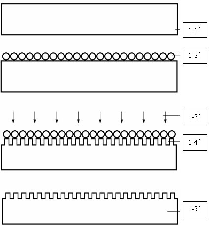
[0014] a) First place the Si substrate ( Picture 1-1 ') in NH 4 OH, H 2 o 2 、H 2 O mixed solution (volume ratio 1:2:6) boiled for 5 minutes, then rinse thoroughly with deionized water;

[0015] b) Dry the cleaned Si substrate and soak it in a 10% sodium dodecyl sulfate solution for 15 hours to obtain a hydrophilic substrate surface; configure a certain amount of polystyrene beads into a colloid Solution, diluted with an equal volume of ethanol, the particle size of the polystyrene beads in it is 200 nm, and the standard deviation is less than 10%; then the diluted solution is dropped on the surface of the soaked Si substrate, the solvent together with the polystyrene Ethylene pellets spread out on the surface of the Si substrate;

[0016] c) Slowly im...

Embodiment 2

[0020] Embodiment 2: Utilize the printing method to cover polystyrene balls on the silicon wafer as a mask layer

[0021] (1) Spread the dense polystyrene beads evenly on the surface of the silicon wafer by printing to form a mask layer containing polystyrene particles: the particle size of the polystyrene beads is 200 nm, and the standard deviation is less than 10%;

[0022] (2) Etching the silicon wafer with the existing mask layer by plasma etching method to form a specific anti-reflection structure;

[0023] (3) Remove the remaining mask layer material on the surface of the silicon wafer.

Embodiment 3

[0024] Example 3: Using printing to cover other regular-shaped polystyrene particles as a mask layer on a silicon wafer

[0025] (1) Spread other regular-shaped polystyrene particles evenly on the surface of the silicon wafer by printing to form a mask layer containing polystyrene particles: the particle size of the polystyrene particles is 10nm~5μm.

[0026] (2) Etching the silicon wafer with the existing mask layer by plasma etching method to form a specific anti-reflection structure;

[0027] (3) Remove the remaining mask layer material on the surface of the silicon wafer.


PUM

PropertyMeasurementUnit
Particle sizeaaaaaaaaaa
Granularityaaaaaaaaaa

Abstract

The invention provides a method for manufacturing a silicon wafer texture, and the method comprises the following specific steps: (1) forming a mask layer containing polystyrene particles on a silicon wafer by using a water film mode or a printing mode; (2) etching the silicon wafer with the mask layer by using a plasma etching method to form a specific anti-reflection structure; and (3) removingthe rest mask layer substance on the surface of the silicon wafer. The method for manufacturing the silicon wafer texture is a nonchemical method, and can be used for preventing a large amount of acid or alkali chemical substances and protecting the ecological environment. The texture of a monocrystal silicon and a polycrystal silicon can be manufactured through the method which is not limited bymonocrystal and polycrystal, so that the reflectivity is reduced, and the silicon wafer can absorb sunlight as much as possible to improve the conversion efficiency of a solar battery.

Description

technical field [0001] The invention relates to a method for manufacturing silicon chip suede. technical background [0002] Reducing the reflectivity to make the silicon wafer absorb sunlight as much as possible is an effective way to increase the conversion efficiency of solar cells. In the manufacturing process of solar cells today, monocrystalline silicon and polycrystalline silicon use different texturing methods to obtain textured surfaces, which reduce reflectivity to varying degrees. Among them, alkali texturing is generally used to make pyramids to form suede in order to obtain better reflectivity; because single crystal alkali texturing uses a large number of high-concentration lye, isopropanol and other chemical substances, it has an impact on the ecological environment . On the basis of slicing the damaged layer, polycrystalline is further corroded by acid texturing to form deep pits similar to "wormholes" to reduce reflectivity. Since polycrystalline acid tex...

Claims


Application Information

Patent Timeline
IPC IPC(8): H01L31/18C30B33/10G02B1/118
CPCY02P70/50
Inventor 解柔强高鹏
Owner MAANSHAN SUPERIOR PV
Why Eureka
Try Eureka