Light-emitting diode (LED) with indium tin oxide (ITO)/zinc oxide based composite transparent electrode and preparation method of LED

A technology of light-emitting diodes and transparent electrodes, which is applied in circuits, electrical components, semiconductor devices, etc., can solve the problems of indium toxicity and complicated process, and achieve the effect of low cost, simple preparation process, and good ohmic contact

Inactive Publication Date: 2011-08-31
SHANGHAI UNIV
View PDF1 Cites 18 Cited by
  • Summary
  • Abstract
  • Description
  • Claims
  • Application Information

AI Technical Summary

Problems solved by technology

[0006] In order to achieve the above-mentioned purpose, the idea of ​​the present invention is to improve the use of zinc oxide with high transmittance, good doping conductivity, and abundant resources in view of the current shortage of indium resources, toxicity of indium, and complicated processes in LEDs. The current expansion layer, in order to form a good ohmic contact with the surface of p-type gall

Method used


Image

  • Light-emitting diode (LED) with indium tin oxide (ITO)/zinc oxide based composite transparent electrode and preparation method of LED
  • Light-emitting diode (LED) with indium tin oxide (ITO)/zinc oxide based composite transparent electrode and preparation method of LED
  • Light-emitting diode (LED) with indium tin oxide (ITO)/zinc oxide based composite transparent electrode and preparation method of LED

Examples


Embodiment 1

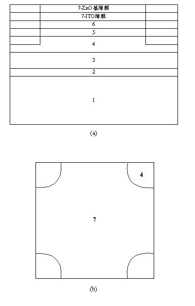
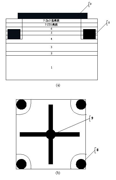
[0027] Embodiment one: see figure 1 and figure 2 , the ITO / ZnO-based transparent electrode light-emitting diode includes: a buffer layer 2, an intrinsic layer 3, an n-type gallium nitride 4, a quantum well 5, a p-type gallium nitride 6 and a transparent electrode on a sapphire substrate 1 in sequence. 7. An n-type metal electrode (PAD) 8 is connected to the n-type gallium nitride 4, and a p-type metal electrode (PAD) 9 is connected to the transparent electrode 7. The buffer layer 2, the intrinsic layer 3, the n-type gallium nitride 4, the quantum well 5, and the p-type gallium nitride 6 are sequentially grown in MOCVD; the transparent electrode 7 is an ITO / zinc oxide composite transparent electrode , where the material of the ITO film is Sn 2 o 3 :In 2 o 3 =1:9 indium tin oxide, the material of the zinc oxide-based transparent conductive film is ZnO:Ga or ZnO:Al or ZnO:In; the n-type metal electrode (8) is a metal composite electrode, and the material is Ti / Al or Cr / Pt...

Embodiment 2

[0028] Embodiment 2: This embodiment is basically the same as Embodiment 1. The special feature is: the special shape of the p-type electrode: a positive cross shape. The p-type metal electrode 9 of this shape makes the current spread more uniform and improves the LED chip. reliability.

Embodiment 3

[0029] Embodiment three: the manufacturing method of the transparent electrode light-emitting diode chip is as follows: first, buffer layer 2, intrinsic layer 3, n-type gallium nitride 4, quantum well 5, p-type gallium nitride are successively formed on the substrate by MOCVD method 6; followed by magnesium activation annealing treatment on the epitaxial wafer; then use chemical reagents such as KOH or HCl or aqua regia to carry out surface treatment on the epitaxial wafer, deposit ITO transparent conductive film by electron beam evaporation, and then pass radio frequency magnetron sputtering The ITO / ZnO-based composite transparent electrode 7 is formed by irradiating the zinc oxide transparent conductive film. The composite transparent electrode is etched into the required pattern by wet etching, and then the n-type gallium nitride is etched by ion etching or ICP etching. Exposed and annealed; deposit n-type metal electrodes (PAD) 8 and p-type metal electrodes (PAD) 9 by therm...


PUM


Abstract

The invention relates to a light-emitting diode (LED) with an indium tin oxide (ITO)/zinc oxide based composite transparent electrode and a manufacturing process of the LED. The LED comprises a buffer layer, an intrinsic layer, an n-gallium nitride (GaN), a quantum well, a p-GaN and an ITO/zinc oxide based composite current expansion layer which are arranged on a sapphire substrate; an n-metal electrode (PAD) is connected with the n-GaN; and a p-metal electrode (PAD) is connected with the ITO/zinc oxide based composite current expansion layer. The manufacturing process comprises the following steps of: finishing sequential growth of the buffer layer, the intrinsic layer, the n-GaN, the quantum well and the p-GaN in metal organic chemical vapour deposition (MOCVD) equipment; sequentially depositing an ITO film and a zinc oxide film on a surface of the p-GaN by electron beam evaporation and magnetron sputtering to form the ITO/zinc oxide based composite current expansion layer; exposing the n-GaN by dry etching; and growing the metal electrodes by thermal evaporation after annealing. The size of a chip is 1mm*1mm. The composite transparent electrode improves contact between the p-GaN and an electrode layer, improves the light extraction efficiency of an LED chip and improves the reliability of the LED chip.

Description

technical field [0001] The invention relates to a light-emitting diode chip and a preparation method thereof, in particular to an ITO / zinc oxide-based composite transparent electrode light-emitting diode and a preparation method thereof. Background technique [0002] Theoretically, the luminous efficiency of LED can be as high as 200lm / W or more, but the current white LED is only about 100lm / W, which is still far behind energy-saving fluorescent lamps; and its price is also at a great disadvantage compared with traditional light sources. There are two main ways to improve the luminous efficiency of LEDs: 1) Improve the internal quantum efficiency of LED chips; 2) Improve the external quantum efficiency of LED chips. At present, the internal quantum luminous efficiency of ultra-high-brightness LEDs has been greatly improved, reaching a maximum of 80%, and there is little room for further improvement. Therefore, improving the external quantum efficiency of LED chips is the ke...

Claims


Application Information

Patent Timeline
IPC IPC(8): H01L33/42H01L33/00
Inventor 王万晶张建华李喜峰
Owner SHANGHAI UNIV
Why Eureka
Try Eureka