RFLDMOS (Radio Frequency Laterally Diffused Metal Oxide Semiconductor) based on self-aligned silicide and tungsten plug structure and manufacturing method thereof
A self-aligned silicide and metal silicide technology, which is used in semiconductor/solid-state device manufacturing, semiconductor devices, electrical components, etc., can solve the problems of increased contact resistance and reduced performance of power chips, and can reduce contact resistance, increase power gain, the effect of improving device performance
- Summary
- Abstract
- Description
- Claims
- Application Information
AI Technical Summary
Problems solved by technology
Method used
Image

Examples
Embodiment
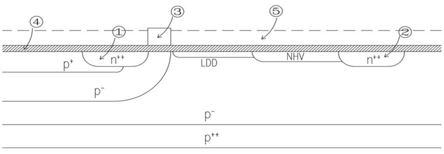
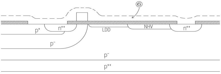
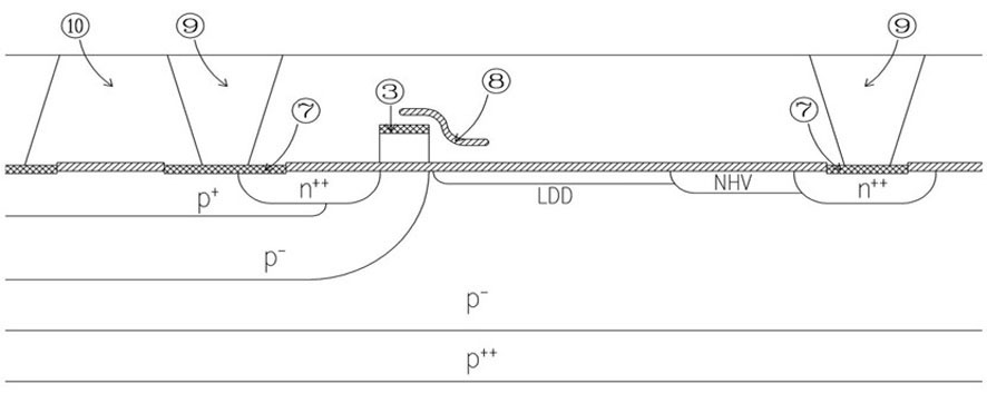
[0025] Example: see figure 1 as shown, figure 1 It is the RFLDMOS cross-sectional view of the polysilicon gate that has been fabricated, in which 1 is the source highly doped region, 2 is the drain highly doped region, 3 is the polysilicon gate, the height is about 2000-3000 Angstroms, and 4 is the surface oxide layer . After the surface oxide layer 4 is removed by wet cleaning, it is filled with SOG solution 5 (Spin On Glass, composed of 80% solvent and 20% silicon dioxide, the ratio can be adjusted according to the actual situation) and evenly spin-coated on the On the surface of the silicon wafer, the height of the solution is slightly lower than the polysilicon gate 3. After the solution is deposited, the SOG is baked to evaporate the solvent. At this time, the entire surface of the silicon wafer is filled with a thin layer of Silicon dioxide; the next step is to etch away part of the oxide layer on the top of the source 1 and the top of the drain 2, and then deposit a l...
PUM
 Abstract
Description
Claims
Application Information
 - Generate Ideas
- Intellectual Property
- Life Sciences
- Materials
- Tech Scout
- Unparalleled Data Quality
- Higher Quality Content
- 60% Fewer Hallucinations
Browse by: Latest US Patents, China's latest patents, Technical Efficacy Thesaurus, Application Domain, Technology Topic, Popular Technical Reports.
© 2025 PatSnap. All rights reserved.Legal|Privacy policy|Modern Slavery Act Transparency Statement|Sitemap|About US| Contact US: help@patsnap.com