
Method for preparing back incident silicon-based tellurium, cadmium and mercury focal plane anti-reflection film by femto-second laser

A femtosecond laser, mercury cadmium telluride technology, applied in the direction of final product manufacturing, sustainable manufacturing/processing, electrical components, etc., can solve the problems of poor reliability of anti-reflection coating, complicated operation process, etc., achieve small thermal effect, simplify preparation steps , the effect of low damage threshold

Active Publication Date: 2011-09-14
SHANGHAI INST OF TECHNICAL PHYSICS - CHINESE ACAD OF SCI
View PDF5 Cites 6 Cited by
  • Summary
  • Abstract
  • Description
  • Claims
  • Application Information

AI Technical Summary

Problems solved by technology

However, the preparation of the anti-reflection coating needs to be completed by photolithography, dry ion etching or thin film replication technology, the operation process is complicated, and the anti-reflection coating used for the tellurium mercury barrier focal plane still has the problem of poor reliability.

Method used


Image

  • Method for preparing back incident silicon-based tellurium, cadmium and mercury focal plane anti-reflection film by femto-second laser
  • Method for preparing back incident silicon-based tellurium, cadmium and mercury focal plane anti-reflection film by femto-second laser
  • Method for preparing back incident silicon-based tellurium, cadmium and mercury focal plane anti-reflection film by femto-second laser

Examples


Embodiment Construction

[0022] Below in conjunction with accompanying drawing, the specific embodiment of the present invention is described in further detail:

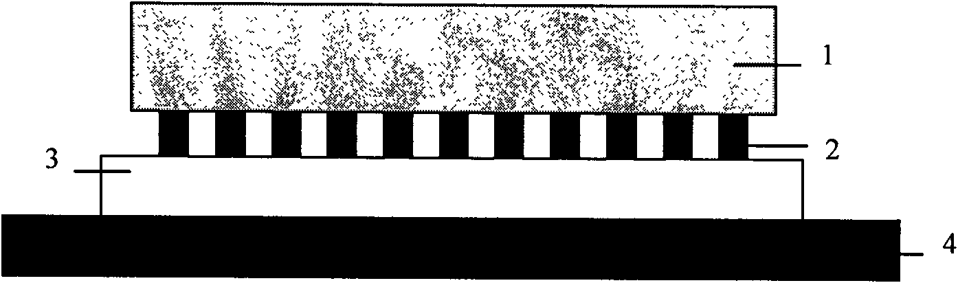
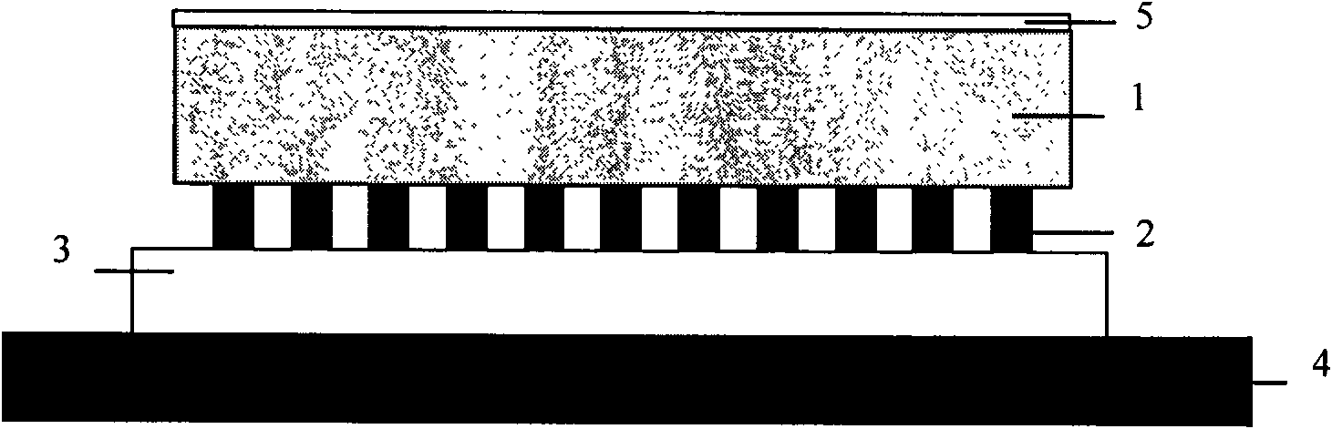
[0023] (1) The silicon-based mercury cadmium telluride infrared detector chip 1 is manufactured by using the conventional mercury cadmium telluride photovoltaic detector manufacturing process, and the chip and the silicon readout circuit 3 are interconnected by the indium column 2 through the cold pressure welding technology and pasted on the gemstone substrate 4 , and finally the prepared focal plane module ( figure 1 ) The chip substrate is placed on the three-dimensional mobile platform facing up.

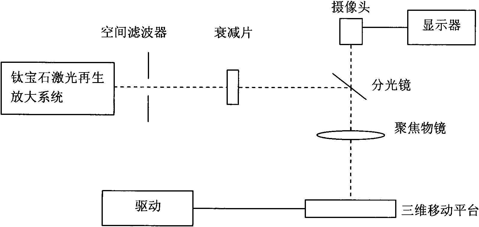
[0024] (2) Using a femtosecond laser to prepare an anti-reflection coating on the chip substrate at the focal plane of HgCdTe, the experimental device is as follows image 3 shown. The titanium sapphire laser regeneration amplification system is used as a light source, outputting laser pulses with a wavelength of 800nm, a pulse width of 60fs...


PUM

PropertyMeasurementUnit
poweraaaaaaaaaa

Abstract

The invention discloses a method for preparing a back incident silicon-based tellurium, cadmium and mercury focal plane anti-reflection film by femto-second laser, and relates to a manufacturing technology for photoelectric detectors. In the method, the anti-reflection film is prepared on the surface of a silicon substrate directly by using a femto-second laser hyperfine 'cold' processing technology; and an appropriate working environment is selected, the appearance of a microstructure is controlled by adjusting parameters such as average power, laser scanning speed and the like of the femto-second laser, and the incident light reflection of the substrate surface is reduced, so that the aim of anti-reflection in an infrared waveband is fulfilled. The anti-reflection film is formed by reconstructing a substrate material under the action of the femto-second laser, so the anti-reflection film has good heat matching with the substrate, and the reliability is high. The femto-second laser hyperfine 'cold' processing method used for preparing the anti-reflection film is simple to operate, and has the advantages of high processing precision and small heat effect, and is particularly suitable for the processing technology of tellurium, cadmium and mercury devices.

Description

technical field [0001] The invention relates to a method for manufacturing an anti-reflection film of a photodetector device, in particular to a method for preparing a back-incident silicon-based mercury cadmium telluride infrared focal plane anti-reflection film by using a femtosecond laser. Background technique [0002] Mercury cadmium telluride material is an ideal infrared detector material, which has the advantages of adjustable band gap, high internal quantum efficiency, and high mobility of electrons and holes. With the wide application of infrared imaging detection technology in military, aerospace, medical and other fields, the development of the third-generation infrared detection system poses new challenges to mercury cadmium telluride infrared focal plane detectors. In order to meet the longer detection distance and higher spatial resolution of the infrared detection system, the pixel scale of the focal plane detector needs to be further expanded. With the wide ...

Claims


Application Information

Patent Timeline
Patent Type & Authority Applications(China)
IPC IPC(8): H01L31/18G02B1/11
CPCY02P70/50
Inventor 张姗胡晓宁廖洋于晓明
Owner SHANGHAI INST OF TECHNICAL PHYSICS - CHINESE ACAD OF SCI
Learn More