Trench-type insulated gate bipolar transistor (Trench IGBT) with enhanced internal conductivity modulation

A bipolar transistor and conductance modulation technology, applied in circuits, electrical components, semiconductor devices, etc., can solve the problems of wasting chip area, reducing chip surface utilization, reducing cell density, etc., and achieve a good forward conduction voltage drop. , optimize the carrier concentration distribution, the effect of electron and hole concentration increase

Inactive Publication Date: 2011-09-28
INST OF ELECTRONICS & INFORMATION ENG IN
View PDF2 Cites 23 Cited by
  • Summary
  • Abstract
  • Description
  • Claims
  • Application Information

AI Technical Summary

Problems solved by technology

However, due to the reduction of cell density, the utilization rate

Method used


Image

  • Trench-type insulated gate bipolar transistor (Trench IGBT) with enhanced internal conductivity modulation
  • Trench-type insulated gate bipolar transistor (Trench IGBT) with enhanced internal conductivity modulation
  • Trench-type insulated gate bipolar transistor (Trench IGBT) with enhanced internal conductivity modulation

Examples


Embodiment Construction

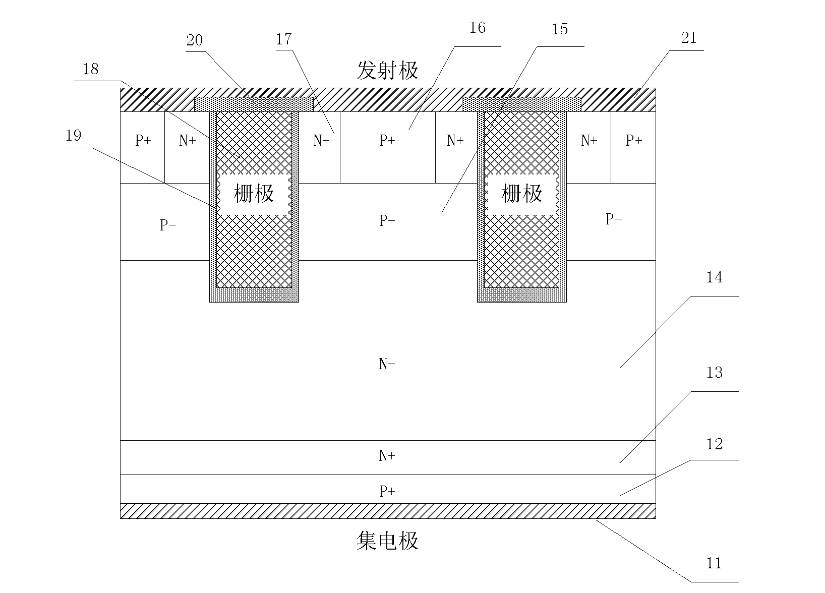
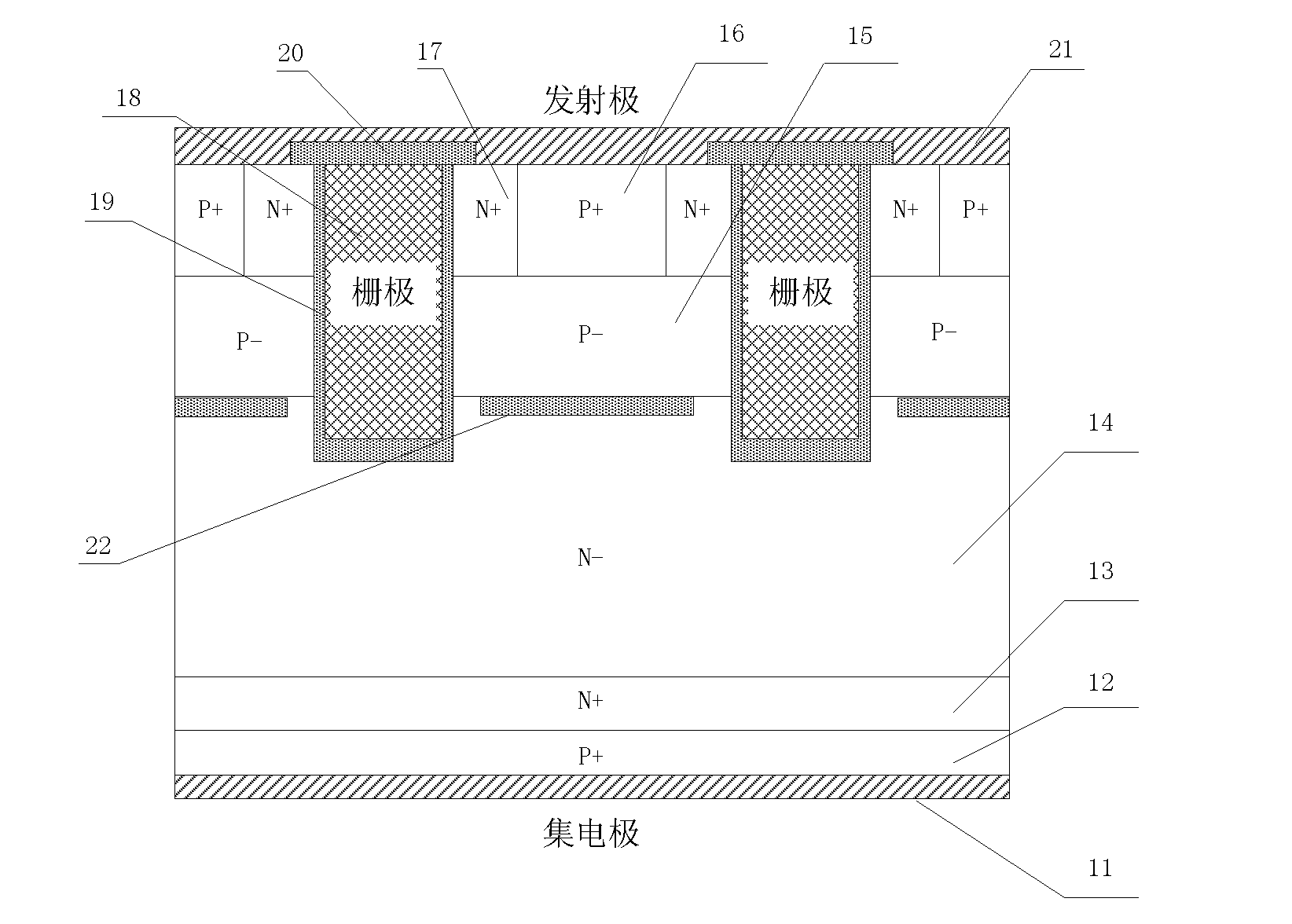
[0020] A trench-type insulated gate bipolar transistor with enhanced conductance modulation in the body, such as image 3 shown, including the collector 11, P + Collector area 12, N + Electric field stop area 13, N - Drift zone 14, P - Base 15, P + Contact zone 16, N + Source region 17, polysilicon gate 18, gate oxide layer 19, insulating layer 20 between gate and emitter and emitter 21; collector 11 is located at P + Backside of collector area 12, N + The electric field cut-off region 13 is located at P + Collector area 12 front, N - Drift region 14 is located at N + The surface of the electric field stop region 13, P + contact area 16 and N + The source regions 17 are located side by side and alternately below the emitter 21 and connected to the emitter 21, P + contact area 16 and N + source region 17 both with N - between the drift region 14 with P - The base region 15; the trench gate electrode structure is located under the emitter 21 and passes through the ...


PUM


Abstract

The invention relates to a Trench IGBT with enhanced internal conductivity, belonging to the technical field of power semiconductor device. According to the invention, on the basis of the structure of the conventional Trench IGBT device, a dielectric layer is introduced between a P<-> base region and an N<-> drift region of the device so as to effectively prevent the P<-> base region from extracting minority carrier holes at the edge of the N<-> drift region during forward conduction, thereby greatly increasing electrons and hole density of the whole N<-> drift region, optimizing the density distribution of carriers in the drift region, enhancing the conductivity modulation in the device, lowering the forward conduction voltage drop of the device, and better compromising the forward conduction voltage drop and the turn-off loss. Meanwhile, the chip surface utilization rate is not reduced and the chip area is saved. The Trench IGBT is suitable for the field of semiconductor power devices and power integrated circuits from small power to large power.

Description

technical field [0001] The invention belongs to the technical field of power semiconductor devices, and relates to a trench type insulated gate bipolar transistor (Trench IGBT), more specifically, relates to a Trench IGBT device with in-body conductance modulation enhancement. Background technique [0002] Power electronics technology with power devices and power integrated circuits as the core and foundation is the key technology to achieve high efficiency and energy saving and promote mechatronics. It is a bridge between weak current control and strong current operation, and between information technology and advanced manufacturing technology. In the field of power electronics, power semiconductor devices are key components, and their characteristics play a vital role in the realization and improvement of system performance. IGBT is a new type of power electronic device combining MOS field effect and bipolar transistor. It not only has the advantages of easy driving of MO...

Claims


Application Information

Patent Timeline
IPC IPC(8): H01L29/739H01L29/06
Inventor 张金平李泽宏安俊杰张波
Owner INST OF ELECTRONICS & INFORMATION ENG IN
Why Eureka
Try Eureka