Photoelectrode material of nanometer porous metal load semiconductor and preparation method thereof

A nanoporous, electrode material technology, applied in the field of photoelectrochemistry, to achieve the effect of inhibiting photocorrosion and excellent performance

Inactive Publication Date: 2011-09-28
SHANDONG UNIV
View PDF5 Cites 15 Cited by
  • Summary
  • Abstract
  • Description
  • Claims
  • Application Information

AI Technical Summary

Problems solved by technology

[0005] After retrieval, this kind of nanoporous metal (gold, titanium, silver, copper, platinum, nickel, aluminum, manganese, cobalt, iron and their alloys) that can be used for solar cells

Method used


Image

  • Photoelectrode material of nanometer porous metal load semiconductor and preparation method thereof
  • Photoelectrode material of nanometer porous metal load semiconductor and preparation method thereof
  • Photoelectrode material of nanometer porous metal load semiconductor and preparation method thereof

Examples


Embodiment 1

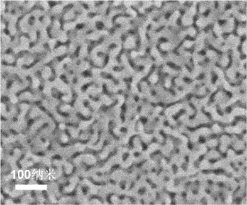
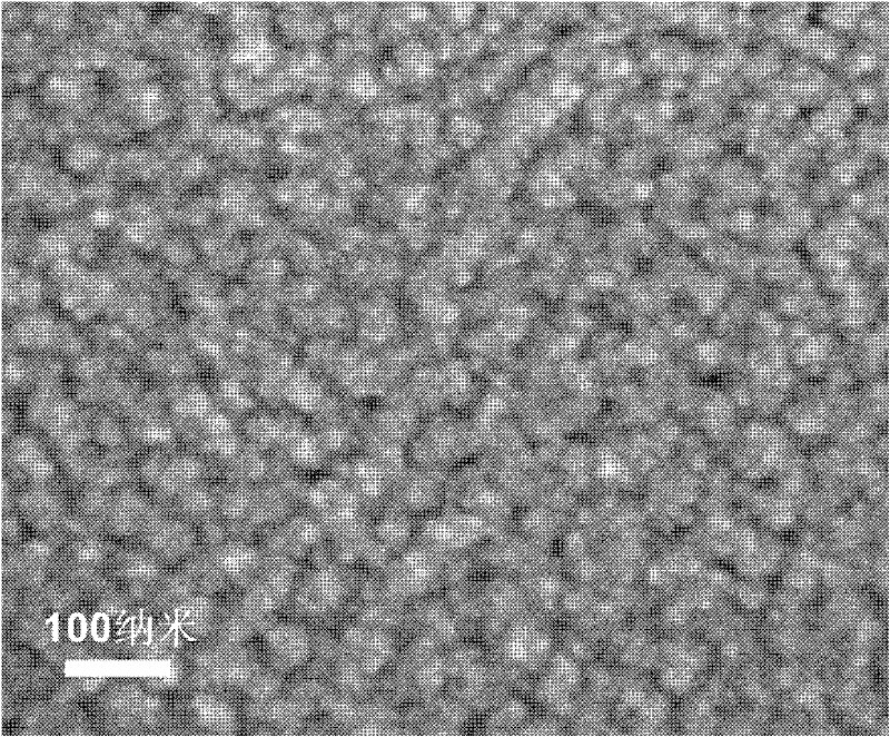
[0043] A nanoporous gold-loaded cadmium sulfide (film or quantum dot) photoelectrode material, comprising nanoporous gold with a thickness of 100 nanometers and a cadmium sulfide layer with a thickness of 5-15 nanometers, the semiconductor layer is evenly covered on the nanometer after deposition. Porous gold has a three-dimensional continuous pore wall surface, and a nanoporous gold-loaded semiconductor photoelectrode material with a pore diameter of 10-50 nanometers, a thickness of 100 nanometers, a width of 1 cm, and a length of 1 cm is prepared, which is a nanoporous structure with three-dimensional continuous openings.

[0044] The preparation method of the photoelectrode material of the above-mentioned nanoporous gold-loaded semiconductor, the steps are as follows:

[0045] (1) be that the thickness is 100 nanometers, width is 1 centimeter, and the nanoporous gold that length is 1 centimeter is placed in the dimethyl sulfoxide solution of 0.05 mol / liter of cadmium nitrate...

Embodiment 2

[0050] A preparation method of a nanoporous gold-loaded cadmium sulfide semiconductor photoelectrode material, the steps are as follows:

[0051] (1) be that the thickness is 100 nanometers, width is 1 centimeter, and the nanoporous gold that length is 1 centimeter is placed in the dimethyl sulfoxide solution of 0.05 mol / liter of cadmium nitrate and 0.1 mol / liter of sulfur that have been deoxygenated;

[0052] (2) Depositing cadmium sulfide on the surface of nanoporous gold under a constant current of 0.0005 ampere for 50 seconds to prepare a nanoporous gold-loaded cadmium sulfide semiconductor photoelectrode material.

[0053] The above nanoporous gold-loaded cadmium sulfide semiconductor photoelectrode material includes nanoporous gold with a thickness of 100 nanometers and a cadmium sulfide semiconductor layer with a thickness of 2-7 nanometers. After the semiconductor layer is deposited, it is uniformly covered on the nanoporous gold three-dimensional continuous On the sur...

Embodiment 3

[0055] A preparation method of a nanoporous gold-loaded cadmium sulfide semiconductor photoelectrode material, the steps are as follows:

[0056] (1) be that the thickness is 100 nanometers, width is 1 centimeter, and the nanoporous gold that length is 1 centimeter is placed in the dimethyl sulfoxide solution of 0.05 mol / liter of cadmium nitrate and 0.1 mol / liter of sulfur that have been deoxygenated;

[0057] (2) Under a constant current of 0.0005 ampere, deposit cadmium sulfide on the surface of nanoporous gold for 110 s to prepare a nanoporous gold-loaded cadmium sulfide semiconductor photoelectrode material.

[0058] The above nanoporous gold-loaded cadmium sulfide semiconductor photoelectrode material includes nanoporous gold with a thickness of 100 nanometers and a cadmium sulfide semiconductor layer with a thickness of 5-13 nanometers. After the semiconductor layer is deposited, it is uniformly covered on the nanoporous gold three-dimensional continuous On the surface o...


PUM

PropertyMeasurementUnit
Thicknessaaaaaaaaaa
Thicknessaaaaaaaaaa
Apertureaaaaaaaaaa

Abstract

The invention relates to a photoelectrode material used in a solar cell and a preparation method thereof, especially relates to a photoelectrode material of a nanometer porous metal load semiconductor and a preparation method thereof, belonging to the photoelectrode chemistry technical field. The photoelectrode material of a nanometer porous metal load semiconductor comprises a nanometer porous metal with a thickness of 50 nanometer to 100 micrometer and a semiconductor layer with a thickness of 1 nanometer to 1 micrometer, wherein after deposition the semiconductor layer uniformly coats the three dimensionally continuous hole wall surface of the nanometer porous metal. Compared with the photoanode material of traditional quantum dot solar cell, nanometer porous metal of the photoelectrode material used in solar cell produced in the invention has a three dimensional porous structure which provides better electrical transmission approach for material.

Description

technical field [0001] The invention relates to a photoelectrode material for solar cells and a preparation method thereof, in particular to a nanoporous metal-loaded semiconductor photoelectrode material and a preparation method thereof, belonging to the field of photoelectrochemical technology. Background technique [0002] With the rapid development of society, the main energy sources used by human beings, such as oil, coal, and natural gas, are gradually depleting, which makes people realize the urgency of seeking new renewable energy sources. As a clean, safe and inexhaustible energy source, solar energy has become a research hotspot, and various solar cells have developed rapidly. Traditional photoelectrochemical cells can no longer meet people's needs, and the high photogenerated electron-hole recombination rate and low photoelectric conversion efficiency have become their biggest obstacles, which has prompted people to devote themselves to the development of next-gen...

Claims


Application Information

Patent Timeline
IPC IPC(8): H01L31/0224H01L31/18
CPCY02P70/50
Inventor 丁轶毕璇璇
Owner SHANDONG UNIV
Why Eureka
Try Eureka