Photoelectrode material of nanometer porous metal load semiconductor and preparation method thereof
A nanoporous and electrode material technology, applied in the field of photoelectrochemistry, to achieve excellent performance and inhibit photocorrosion
- Summary
- Abstract
- Description
- Claims
- Application Information
AI Technical Summary
Problems solved by technology
Method used
Image
Examples
Embodiment 1
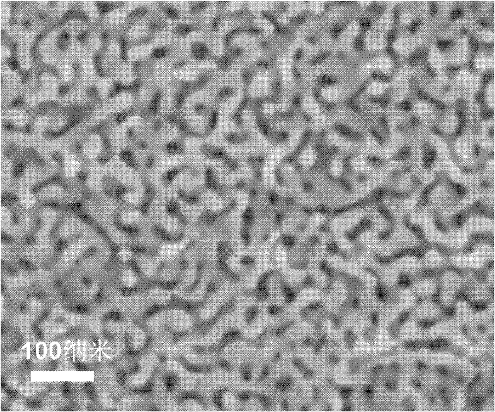
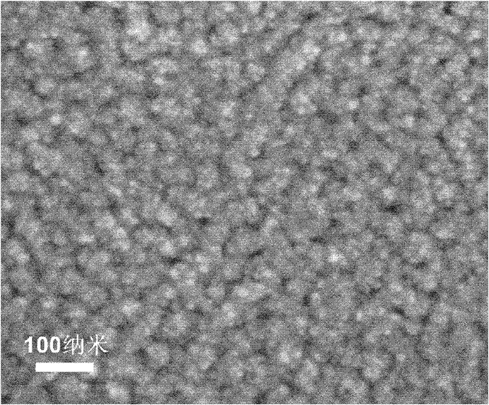
[0043] A nanoporous gold-loaded cadmium sulfide (film or quantum dot) photoelectrode material, comprising nanoporous gold with a thickness of 100 nanometers and a cadmium sulfide layer with a thickness of 5-15 nanometers, the semiconductor layer is evenly covered on the nanometer after deposition. Porous gold has a three-dimensional continuous pore wall surface, and a nanoporous gold-loaded semiconductor photoelectrode material with a pore diameter of 10-50 nanometers, a thickness of 100 nanometers, a width of 1 cm, and a length of 1 cm is prepared, which is a nanoporous structure with three-dimensional continuous openings.
[0044] The preparation method of the photoelectrode material of the above-mentioned nanoporous gold-loaded semiconductor, the steps are as follows:
[0045] (1) be that the thickness is 100 nanometers, width is 1 centimeter, and the nanoporous gold that length is 1 centimeter is placed in the dimethyl sulfoxide solution of 0.05 mol / liter of cadmium nitrate...
Embodiment 2
[0050] A preparation method of a nanoporous gold-loaded cadmium sulfide semiconductor photoelectrode material, the steps are as follows:
[0051] (1) be that the thickness is 100 nanometers, width is 1 centimeter, and the nanoporous gold that length is 1 centimeter is placed in the dimethyl sulfoxide solution of 0.05 mol / liter of cadmium nitrate and 0.1 mol / liter of sulfur that have been deoxygenated;
[0052] (2) Depositing cadmium sulfide on the surface of nanoporous gold under a constant current of 0.0005 ampere for 50 seconds to prepare a nanoporous gold-loaded cadmium sulfide semiconductor photoelectrode material.
[0053] The above nanoporous gold-loaded cadmium sulfide semiconductor photoelectrode material includes nanoporous gold with a thickness of 100 nanometers and a cadmium sulfide semiconductor layer with a thickness of 2-7 nanometers. After the semiconductor layer is deposited, it is uniformly covered on the nanoporous gold three-dimensional continuous On the sur...
Embodiment 3
[0055] A preparation method of a nanoporous gold-loaded cadmium sulfide semiconductor photoelectrode material, the steps are as follows:
[0056] (1) be that the thickness is 100 nanometers, width is 1 centimeter, and the nanoporous gold that length is 1 centimeter is placed in the dimethyl sulfoxide solution of 0.05 mol / liter of cadmium nitrate and 0.1 mol / liter of sulfur that have been deoxygenated;
[0057] (2) Under a constant current of 0.0005 ampere, deposit cadmium sulfide on the surface of nanoporous gold for 110 s to prepare a nanoporous gold-loaded cadmium sulfide semiconductor photoelectrode material.
[0058] The above nanoporous gold-loaded cadmium sulfide semiconductor photoelectrode material includes nanoporous gold with a thickness of 100 nanometers and a cadmium sulfide semiconductor layer with a thickness of 5-13 nanometers. After the semiconductor layer is deposited, it is uniformly covered on the nanoporous gold three-dimensional continuous On the surface o...
PUM
| Property | Measurement | Unit |
|---|---|---|
| thickness | aaaaa | aaaaa |
| pore size | aaaaa | aaaaa |
| thickness | aaaaa | aaaaa |
Abstract
Description
Claims
Application Information
 - R&D
- Intellectual Property
- Life Sciences
- Materials
- Tech Scout
- Unparalleled Data Quality
- Higher Quality Content
- 60% Fewer Hallucinations
Browse by: Latest US Patents, China's latest patents, Technical Efficacy Thesaurus, Application Domain, Technology Topic, Popular Technical Reports.
© 2025 PatSnap. All rights reserved.Legal|Privacy policy|Modern Slavery Act Transparency Statement|Sitemap|About US| Contact US: help@patsnap.com


