Silicon nanowire grating resonant enhanced photoelectric detector and manufacturing method thereof

A photodetector and silicon nanowire technology, applied in circuits, electrical components, semiconductor devices, etc., to achieve the effects of improving quantum efficiency, enhancing light field, and reducing source-drain bias voltage

Inactive Publication Date: 2011-09-28
INST OF SEMICONDUCTORS - CHINESE ACAD OF SCI
View PDF3 Cites 39 Cited by
  • Summary
  • Abstract
  • Description
  • Claims
  • Application Information

AI Technical Summary

Problems solved by technology

In 2008, Islam et al. from the University of California reported a method for preparing a photodetector by using the lateral induced growth method to connect a large number of silicon, InP or Zn0 nanowires in parallel, and obtained a bandwidth of 30 GHz, which is novel, but the nanostructure of the device There are still many challenges in positioning and reliability control (see M.S.Islam et al., 2nd IEEE International Nanoelectronics Conference, 1009-1014, 2008)

Method used


Image

  • Silicon nanowire grating resonant enhanced photoelectric detector and manufacturing method thereof
  • Silicon nanowire grating resonant enhanced photoelectric detector and manufacturing method thereof

Examples


Embodiment

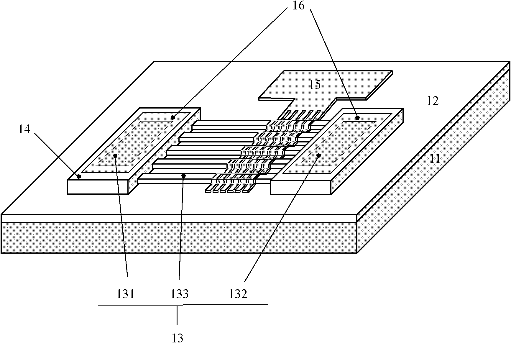
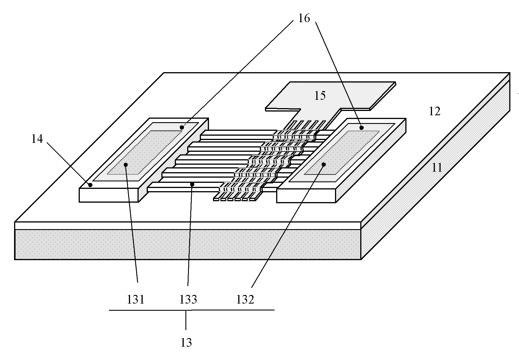
[0052] Please refer to figure 1 According to the invention, a silicon nanowire grating resonance enhanced photodetector can be fully compatible with CMOS technology, and is suitable for the application of optoelectronic hybrid integrated circuit (OEIC).

[0053] First, select a silicon substrate 11 (400 μm)-silicon oxide layer 12 (300nm)-an SOI (or SIMOX) sheet with a thin intrinsic top silicon layer (200nm) structure; thermally oxidize the 200nm-thick top-layer silicon at 900°C to obtain a 30nm-thick Thermal silicon oxide layer; cover the sample with 1 μm thick photoresist AZ6130, and then photo-etch the mask pattern of the I-shaped mesa 13 after pre-baking. After the silicon oxide is etched by ICP, the top silicon thin layer is etched by ICP. The silicon thin layer forms the I-shaped mesa 13 . Next, cover the sample with a 200nm thick photoresist PMMA950K, and dry it on a hot plate at 180°C for 90 seconds; use an electron beam exposure sleeve to carve out the mask layer of ...


PUM

PropertyMeasurementUnit
thicknessaaaaaaaaaa

Abstract

The invention discloses a silicon nanowire grating resonant enhanced photoelectric detector, which comprises a silicon substrate, a silicon oxide layer, an I-shaped mesa structure, a protective layer, a metal gate electrode and two photocurrent output metal electrodes, wherein the silicon oxide layer is manufactured on the silicon substrate; the I-shaped mesa structure is manufactured on the silicon oxide layer, two ends of the I-shaped mesa structure are provided with a P-type electrode and an N-type electrode, and a silicon nanowire grating resonant cavity structure is connected between the P-type electrode and the N-type electrode; the protective layer is manufactured on the surface and side faces of the I-shaped mesa structure, and electrode windows are formed on the P-type electrode and the N-type electrode at two ends of the I-shaped mesa structure; the metal gate electrode is manufactured on the protective layer of the silicon nanowire grating resonant cavity structure and is close to one side of the N-type electrode; and the two photocurrent output metal electrodes are manufactured in the electrode windows of the protective layer on the P-type electrode and the N-type electrode of the I-shaped mesa structure.

Description

technical field [0001] The invention relates to the field of nanostructure photodetectors, in particular to a silicon nanowire grating resonance enhanced photodetector and a manufacturing method thereof. Background technique [0002] Silicon is not only an electronic material, but also a photonic material. Very mature microelectronics processing technology has provided solid technical support for silicon photonics, greatly accelerating the formation and development of silicon photonics. In the past few decades, silicon processing capabilities have already entered the submicron range smaller than the wavelength of light, and are developing towards the nanoscale range. Silicon nanophotonics is and has become the most exciting new frontier today. Silicon nanophotonics, which deals with the interaction of light and matter in the nanometer range shorter than the wavelength, creates exciting opportunities and enables the development of new technologies. [0003] Due to the nano...

Claims


Application Information

Patent Timeline
Patent Type & Authority Applications(China)
IPC IPC(8): H01L31/105H01L31/0352B81C1/00H01L31/18
CPCY02P70/50
Inventor 韩伟华陈燕坤李小明张严波杜彦东杨富华
Owner INST OF SEMICONDUCTORS - CHINESE ACAD OF SCI
Why Eureka
Try Eureka