
AlGan polarized ultraviolet photoelectric detector and manufacturing method thereof
A technology of electric detector and ultraviolet light, which is applied in the field of microelectronics, can solve the problems of thinning of the active area, large dark current, and restriction of detection performance, and achieve fast migration rate, reduce dark current, and improve high-frequency characteristics Effect
- Summary
- Abstract
- Description
- Claims
- Application Information
AI Technical Summary
Problems solved by technology
Method used
Image

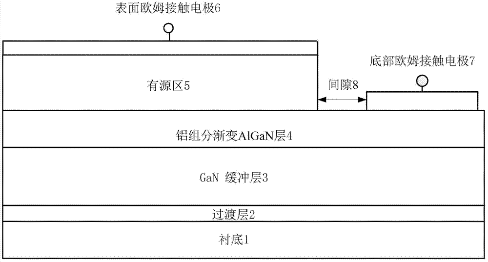
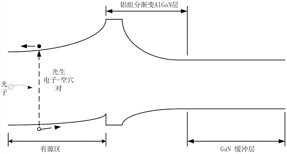
Examples
Embodiment 1
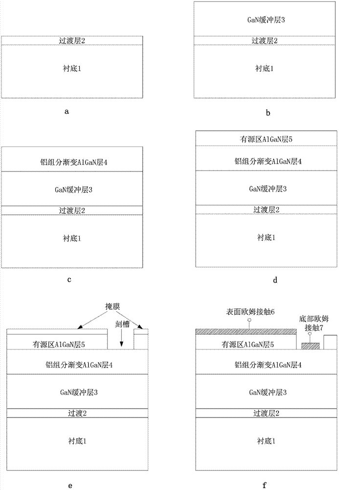
[0030] Step 1, epitaxially grow transition layer 2 on substrate 1, such as image 3 a.
[0031] Using metal-organic chemical vapor deposition technology, grow an AlN transition layer 2 with a thickness of 10nm on the sapphire substrate 1 to release the stress caused by lattice mismatch. The growth process conditions are as follows: temperature is 990°C, pressure is 122 Torr, the flow rate of hydrogen gas is 4400 sccm, the flow rate of ammonia gas is 4400 sccm, and the flow rate of aluminum source is 6 μmol / min.
[0032] Step 2, depositing a GaN buffer layer 3 on the transition layer 2, such as image 3 b.
[0033] Using metal-organic chemical vapor deposition technology, a GaN buffer layer 3 with a thickness of 2 μm is grown on the transition layer 2. The GaN surface is required to be flat and there is no stress accumulation caused by lattice mismatch. The process conditions are: the temperature is 990°C , the pressure is 122 Torr, the flow rate of hydrogen gas is 4400 sccm, ...
Embodiment 2
[0043] Step 1, epitaxially grow transition layer 2 on substrate 1, such as image 3 a.
[0044] A buffer layer 2 made of AlN with a thickness of 5nm is grown on a silicon carbide substrate 1 by metal-organic chemical vapor deposition technology to release the stress caused by lattice mismatch. Process conditions: temperature is 990°C, pressure is 122Torr, hydrogen The flow rate is 4400 sccm, the flow rate of ammonia gas is 4400 sccm, and the flow rate of aluminum source is 6 μmol / min;
[0045] Step 2, depositing a GaN buffer layer 3 on the transition layer 2, such as image 3 b.
[0046] This step is the same as Step 2 of Embodiment 1.
[0047] Step 3, making an aluminum composition graded AlGaN layer 4 on the barrier layer 3, such as image 3 c.
[0048] Using metal-organic chemical vapor deposition technology, 25nm aluminum composition graded AlGaN is first deposited on the GaN buffer layer 3, and its aluminum composition increases from 0% to 90%. The process conditions...
Embodiment 3
[0056] Step 1, epitaxially grow transition layer 2 on substrate 1, such as image 3 a.
[0057] Using metal-organic chemical vapor deposition technology, first grow a 5nm thick AlN layer on the silicon substrate 1, the process conditions are: temperature 1040°C, pressure 100Torr, hydrogen flow rate 4400sccm, ammonia flow rate 4400sccm, aluminum source flow rate 6μmol / min; then grow 15 cycles of AlGaN / GaN superlattice, the thickness of the GaN potential well is 5nm, the aluminum composition of the AlGaN barrier layer is 20%, and the thickness is also 5nm. Process conditions: temperature 1040°C, pressure 100 Torr, hydrogen flow rate 4400 sccm, ammonia gas flow rate 4400 sccm, gallium source flow rate 120 μmol / min, aluminum source flow rate 1.2 μmol / min when growing AlGaN,
[0058] Step 2, depositing a GaN buffer layer 3 on the transition layer 2, such as image 3 b.
[0059] It is the same as Step 2 of Embodiment 1.
[0060] Step 3, making an aluminum composition graded AlGa...
PUM
 Abstract
Description
Claims
Application Information