Preparation method of Ga doped ZnO nanowire catalyzed by Sn
A technology of nanowires and preparation steps, applied in the field of optoelectronic information functional materials, can solve problems such as complex process, and achieve the effects of ensuring luminescence performance, convenient preparation process and high yield
- Summary
- Abstract
- Description
- Claims
- Application Information
AI Technical Summary
Problems solved by technology
Method used
Image

Examples
Embodiment 1
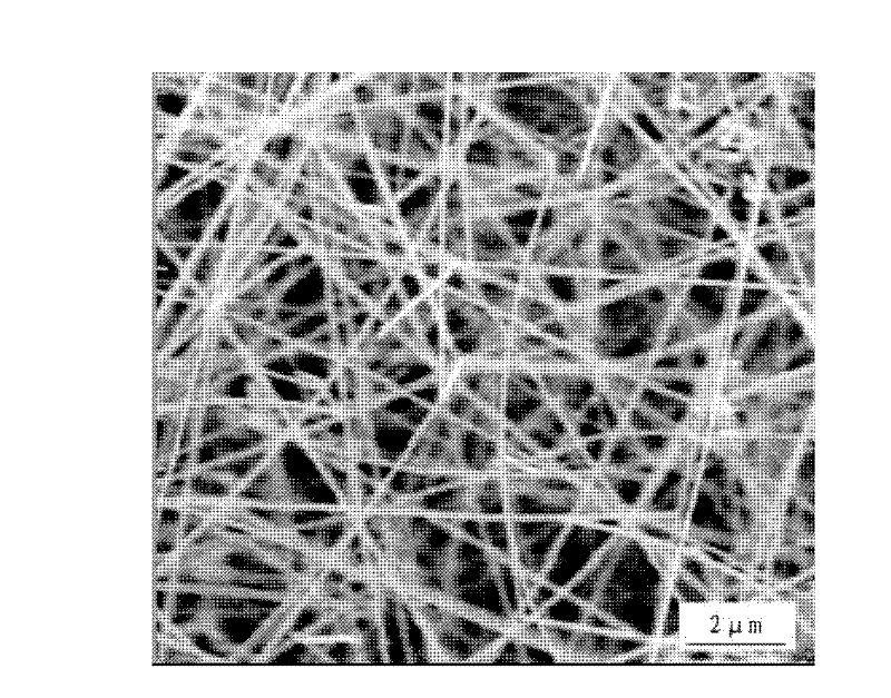
[0015] Clean the alumina boat and dry it, put the Ga droplet in the alumina boat, then evenly mix ZnO powder and Sn powder (weight ratio 10:3) and spread it on the Ga source to cover it. Place the cleaned silicon wafer coated with a film facing down directly above the evaporation source, and the vertical distance between the silicon wafer and the evaporation source is about 6 mm. In order to prevent the silicon wafer from sliding on the alumina boat, Pt wire was used to fix it on the alumina boat. Push the alumina boat equipped with evaporation source and silicon wafer into the tube furnace smoothly, and then fill the tube furnace with argon gas at 200 ml / min for 5 min. At the gas flow outlet, place the vent tube in the water and allow the argon to escape through the water. Raise the temperature of the furnace to 910 °C, keep it warm for 10 min, and fill it with argon with a flow rate of 120 ml / min. Then the tube furnace was naturally cooled to room temperature. Depend on ...
Embodiment 2
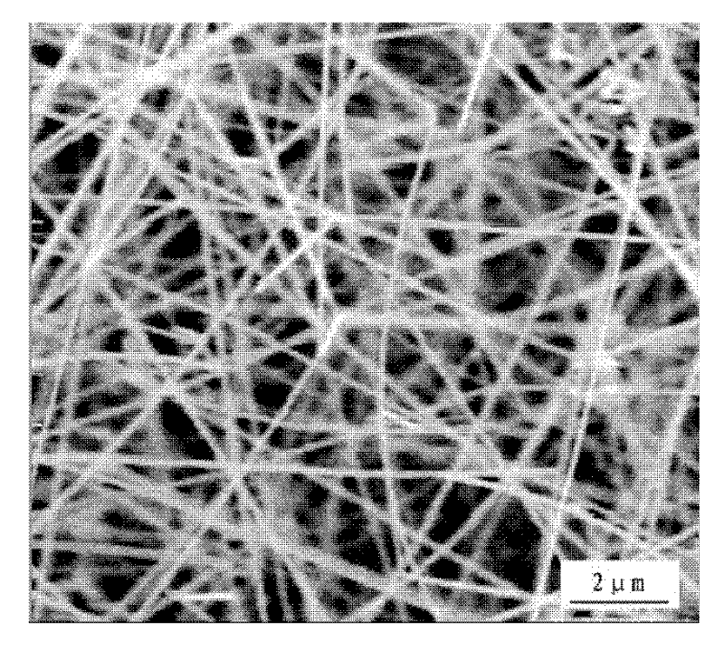
[0017] Clean the alumina boat and dry it, put the Ga droplet in the alumina boat, then evenly mix ZnO powder and Sn powder (weight ratio 10:2) and spread it on the Ga source to cover it. Place the cleaned silicon wafer coated with a film facing down directly above the evaporation source, and the vertical distance between the silicon wafer and the evaporation source is about 5 mm. In order to prevent the silicon wafer from sliding on the alumina boat, Pt wire was used to fix it on the alumina boat. Push the alumina boat equipped with evaporation source and silicon wafer into the tube furnace smoothly, and then fill the tube furnace with argon gas at 200 ml / min for 10 min. At the gas flow outlet, place the vent tube in the water and allow the argon to escape through the water. Raise the temperature of the furnace to 920 °C, keep it warm for 13 min, and fill it with argon with a flow rate of 110 ml / min. Then the tube furnace was naturally cooled to room temperature. The sample...
Embodiment 3
[0019] Clean the alumina boat and dry it, put the Ga droplet in the alumina boat, then evenly mix ZnO powder and Sn powder (weight ratio 10:2.5) and spread it on the Ga source to cover it. Place the cleaned silicon wafer coated with a film facing down directly above the evaporation source, and the vertical distance between the silicon wafer and the evaporation source is about 5 mm. In order to prevent the silicon wafer from sliding on the alumina boat, Pt wire was used to fix it on the alumina boat. Push the alumina boat equipped with evaporation source and silicon wafer into the tube furnace smoothly, and then fill the tube furnace with argon gas at 300 ml / min for 5 min. At the gas flow outlet, place the vent tube in the water and allow the argon to escape through the water. Raise the temperature of the furnace to 880 °C, keep it warm for 15 min, and fill it with argon gas at a flow rate of 100 ml / min. Then the tube furnace was naturally cooled to room temperature. The sam...
PUM
 Abstract
Description
Claims
Application Information
 - R&D
- Intellectual Property
- Life Sciences
- Materials
- Tech Scout
- Unparalleled Data Quality
- Higher Quality Content
- 60% Fewer Hallucinations
Browse by: Latest US Patents, China's latest patents, Technical Efficacy Thesaurus, Application Domain, Technology Topic, Popular Technical Reports.
© 2025 PatSnap. All rights reserved.Legal|Privacy policy|Modern Slavery Act Transparency Statement|Sitemap|About US| Contact US: help@patsnap.com