Check patentability & draft patents in minutes with Patsnap Eureka AI!

Preparing and etching method of plugged-in TiN metal gate lamination structure

A stacked structure and metal gate technology, applied in the direction of semiconductor devices, etc., to achieve the effect of reducing the difficulty of etching, high compatibility, and low loss

Active Publication Date: 2013-08-28
BEIJING YANDONG MICROELECTRONICS
View PDF5 Cites 0 Cited by
  • Summary
  • Abstract
  • Description
  • Claims
  • Application Information

AI Technical Summary

Problems solved by technology

[0003] Although the introduction of Hf-based high-K and metal gate materials can improve the performance of the device, the integration of high-K / metal gate in the gate-first process, especially the etching process of the metal gate stack structure, has always been a high-K, metal One of the main challenges in the practical application of gate materials to CMOS processes

Method used


Image

  • Preparing and etching method of plugged-in TiN metal gate lamination structure
  • Preparing and etching method of plugged-in TiN metal gate lamination structure
  • Preparing and etching method of plugged-in TiN metal gate lamination structure

Examples


Embodiment Construction

[0033] In order to make the object, technical solution and advantages of the present invention clearer, the present invention will be described in further detail below in conjunction with specific embodiments and with reference to the accompanying drawings.

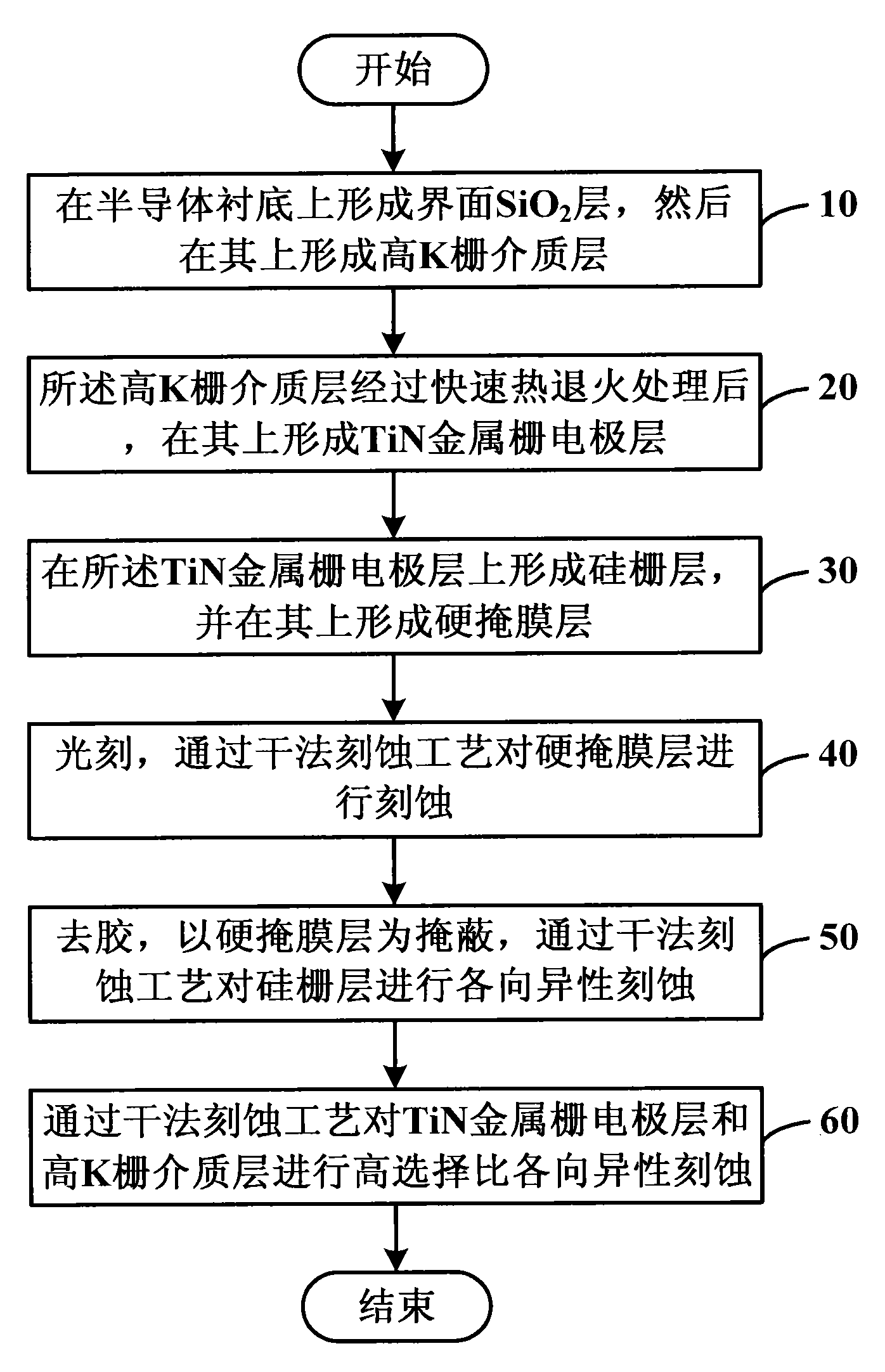
[0034] Such as figure 1 as shown, figure 1 It is a flowchart of a method for preparing and etching an interposed TiN metal gate stack structure provided by the present invention, and the method includes the following steps:

[0035] Step 10: Formation of interfacial SiO on the semiconductor substrate 2 layer, and then form a high-K gate dielectric layer thereon;

[0036] Step 20: forming a TiN metal gate electrode layer on the high-K gate dielectric layer after rapid thermal annealing;

[0037] Step 30: forming a silicon gate layer on the TiN metal gate electrode layer, and forming a hard mask layer thereon;

[0038] Step 40: photolithography, etching the hard mask layer through a dry etching process;

[0039] Step 5...


PUM

PropertyMeasurementUnit
poweraaaaaaaaaa
thicknessaaaaaaaaaa
thicknessaaaaaaaaaa

Abstract

The invention discloses a preparing and etching method of a plugged-in TiN metal gate lamination structure. The preparing and etching method comprises the following steps: forming an interface SiO2 layer on a semiconductor substrate; forming a high-K gate dielectric layer on the interface SiO2 layer; after the high-K gate dielectric layer is subjected to quick thermal annealing treatment, forminga TiN metal gate electrode layer on the high-K gate dielectric layer; forming a silicon gate layer on the TiN metal gate electrode layer; forming a hard mask layer on the silicon gate layer; photoetching: etching the hard mask layer by the dry etching technology; removing photoresist: taking the hard mask layer as a mask, and carrying out anisotropic etching on the silicon gate layer by the dry etching technology; and carrying out anisotropic etching with a high selection ratio on the TiN metal gate electrode layer and the high-K grid dielectric layer by the dry etching technology. According to the preparing and etching method, the preparation requirements of the TiN metal gate and the high-K material in the plugged-in metal gate lamination structure can be satisfied, and a steep etching section can be obtained by optimizing the etching technology of the TiN metal gate and the high-K medium, thereby providing necessary guarantee for the integration of a high-K / metal gate.

Description

technical field [0001] The invention relates to the technical field of integrated circuit manufacturing, in particular to a method for preparing and etching a metal gate stack structure in a gate-first process. Background technique [0002] As the feature size of semiconductor devices enters the 45nm technology node, in order to reduce the gate tunneling current, reduce the power consumption of the device, and completely eliminate the polysilicon depletion effect and P-type metal-oxide-semiconductor field effect transistor (PMOSFET) Reliability issues caused by medium B penetration, alleviate the Fermi level pinning effect, and use high dielectric constant (K) / metal gate materials instead of traditional SiO 2 / Polysilicon (poly) structure has become an inevitable choice. Among many high-K materials, Hf-based high-K materials are finally considered to be the most promising SiO2 materials. 2 Alternatives to gate dielectrics. On the other hand, TiN metal gate material has b...

Claims


Application Information

Patent Timeline
Patent Type & Authority Patents(China)
IPC IPC(8): H01L21/28
Inventor 李永亮徐秋霞
Owner BEIJING YANDONG MICROELECTRONICS
Features
  • R&D
  • Intellectual Property
  • Life Sciences
  • Materials
  • Tech Scout
  • Unparalleled Data Quality
  • Higher Quality Content
  • 60% Fewer Hallucinations
Learn More