Photonic quasicrystal graph sapphire substrate and manufacturing method thereof and light emitting diode and preparation method thereof

A sapphire substrate and light-emitting diode technology, applied in semiconductor devices, electrical components, circuits, etc., can solve the problems of increasing the thermal resistance of LED chips, demanding photolithography technology, and limiting LED optical power, etc., to improve leakage characteristics and Improvement of internal quantum efficiency and light extraction efficiency

Inactive Publication Date: 2011-11-16
JIANGSU E LITE SEMICON
View PDF6 Cites 11 Cited by
  • Summary
  • Abstract
  • Description
  • Claims
  • Application Information

AI Technical Summary

Problems solved by technology

However, photonic crystal pattern substrates still have several disadvantages: First, the geometric dimensions of photonic crystals are all on the sub-micron scale. In addition to demanding photonic technology, voids are easily formed during epitaxial growth, which increases the cost of LED chips. Thermal resistance, which

Method used


Image

  • Photonic quasicrystal graph sapphire substrate and manufacturing method thereof and light emitting diode and preparation method thereof
  • Photonic quasicrystal graph sapphire substrate and manufacturing method thereof and light emitting diode and preparation method thereof
  • Photonic quasicrystal graph sapphire substrate and manufacturing method thereof and light emitting diode and preparation method thereof

Examples


Embodiment 1

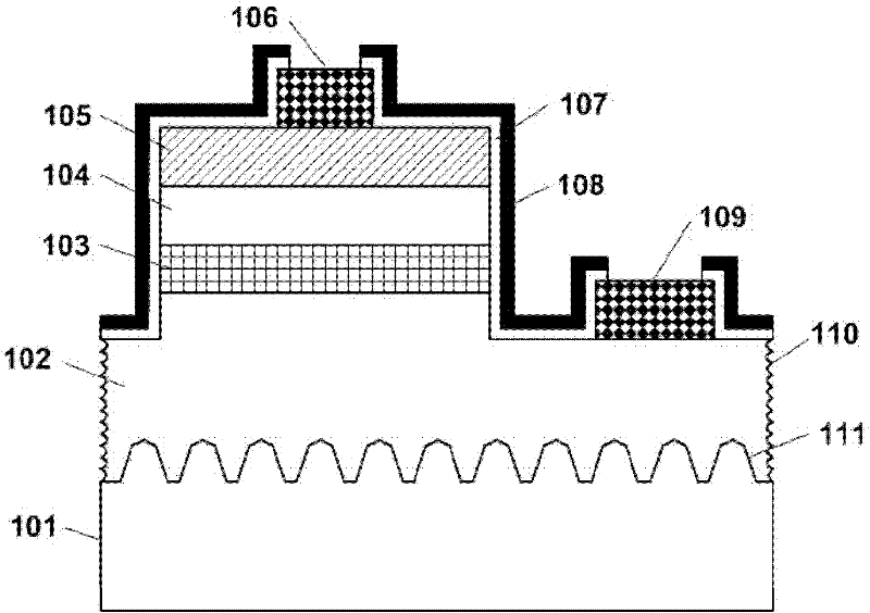
[0042] Such as figure 1 As shown, the light emitting diode structure provided in this embodiment includes: N-type GaN 102 is formed on a sapphire substrate 101; a multi-quantum well layer 103 is formed on N-type GaN 102; P-type GaN 104 is formed on On the multi-quantum well layer 103; the ITO transparent conductive layer 105 is formed on the P-type gallium nitride 104; the P electrode 106 is formed on the ITO transparent conductive layer 105; the N electrode 109 is formed on the N-type gallium nitride 102 The first passivation layer 107 of silicon nitride is formed on the mesa and sidewall of the light-emitting diode; the second passivation layer 108 of silicon nitride oxide is formed on the first passivation layer 107 of silicon nitride; the microstructure 110 of the sidewall is formed on On the sidewall of the N-type gallium nitride 102 ; the quasi-photonic crystal pattern structure 111 is formed on the single crystal sapphire substrate 101 .

[0043] A method of manufactu...


PUM

PropertyMeasurementUnit
Lattice constantaaaaaaaaaa

Abstract

The invention relates to a sapphire substrate and a manufacturing method thereof and a light emitting diode adopting the sapphire substrate and a preparation method thereof. The surface of the sapphire substrate is provided with a graph structure of a photonic quasicrystal structure. The proportion of the area of a C surface of the sapphire substrate, which is exposed in the graph structure, in the whole bottom area of the sapphire substrate is low. The surface of the sapphire substrate is provided with the graph structure of the photonic quasicrystal structure; the graph structure is formed in a mode that sub regions are periodically arrayed and has the lattice constant of 0.2 to 5mum; a space between each two adjacent sub regions is of a V shape or a similar V shape; the sub regions extend to the side wall of the C surface of the sapphire substrate and are at an angle of 25 to 60 degrees with the C surface of the sapphire substrate; and the proportion of the C surface of the sapphire substrate, which is exposed in the graph structure, is lower than 20 percent. The manufacturing method of the sapphire substrate comprises the following steps of: forming the photonic crystal structure on the surface of the sapphire substrate; and then carrying out anisotropic etching on the side wall of the photonic crystal structure by using a phosphoric acid/sulphuric acid mixed solution so as to form the photonic quasicrystal graph structure.

Description

technical field [0001] The invention relates to a sapphire substrate with a quasi-photon crystal pattern and a manufacturing method thereof, a light-emitting diode and a manufacturing method thereof. Background technique [0002] Light-emitting diodes based on III-nitride semiconductor materials (GaN, AlN, InN and their alloys) have the advantages of small size, long life, and high efficiency. They are used in general lighting, traffic indication, outdoor full-color display, LCD backlight, household It has broad application prospects in many fields such as electrical indicator lights. Compared with silicon carbide (SiC) and silicon (Si) substrates, epitaxial GaN-based LED materials on sapphire substrates have the advantages of high technological maturity, low cost, and large-scale production, and have been widely adopted by the industry. [0003] Due to the difference in lattice constant and thermal expansion coefficient between the sapphire substrate and GaN-based LED mate...

Claims


Application Information

Patent Timeline
IPC IPC(8): H01L33/20H01L33/44H01L33/22H01L33/00
Inventor 刘洪刚张雄
Owner JIANGSU E LITE SEMICON
Why Eureka
Try Eureka