Silicon carbide gridding electrode PIN type nuclear battery

A grid-shaped, nuclear battery technology, applied in the field of microelectronics, can solve the problems of reducing energy conversion efficiency, energy loss, etc., and achieve the effect of improving energy conversion efficiency, reducing blocking effect, and being easy to implement

Inactive Publication Date: 2011-12-14
XIDIAN UNIV
View PDF8 Cites 12 Cited by
  • Summary
  • Abstract
  • Description
  • Claims
  • Application Information

AI Technical Summary

Problems solved by technology

In this p-i-n junction structure, in order to prevent the ohmic contact electrode from blocking incident particles, the ohmic electrode must be overloaded in one corner of the device, but this will cause the irradiated carriers far away from the ohmic electrode to be recombined during the transport process, Cause energy loss and reduce energy conversion efficiency

Method used


Image

  • Silicon carbide gridding electrode PIN type nuclear battery
  • Silicon carbide gridding electrode PIN type nuclear battery
  • Silicon carbide gridding electrode PIN type nuclear battery

Examples


Embodiment 1

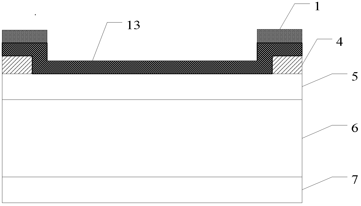
[0039] In the first step, a low-doped n-type epitaxial layer is epitaxially grown on a SiC highly doped n-type substrate sample, such as Figure 6 a.

[0040] The selected doping concentration is 1×10 18 cm -3 After cleaning, the highly doped n-type SiC substrate sample 7 is epitaxially grown on the highly doped n-type SiC substrate sample with a thickness of 3 μm, and the n-type low-doped epitaxial layer 6 doped with nitrogen ions has a doping concentration of 1×10 15 cm -3 , the epitaxy temperature is 1570°C, the pressure is 100mbar, the reaction gas is silane and propane, the carrier gas is pure hydrogen, and the impurity source is liquid nitrogen.

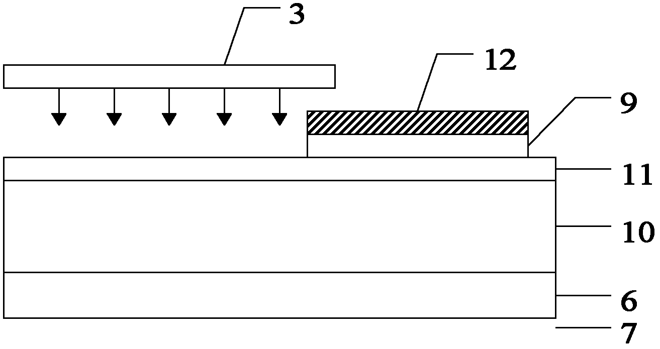
[0041] Step 2: Epitaxial growth of highly doped p-type epitaxial layer, such as Figure 6 b.

[0042] The p-type epitaxial layer 5 doped with aluminum ions is epitaxially grown on the low-doped epitaxial wafer with a thickness of 0.5 μm, and its doping concentration is 2×10 19 cm -3 , the epitaxy temperature is 1570°C, ...

Embodiment 2

[0060] Step 1: Epitaxial low-doped n-type epitaxial layer on the SiC highly doped n-type substrate sample, such as Figure 6 a.

[0061] A highly doped n-type SiC substrate sample 7 is selected, and its doping concentration is 5×10 18 cm -3 , after cleaning, the epitaxial growth thickness of the highly doped n-type SiC substrate sample is 3.5 μm, n-type low-doped epitaxial layer 6 doped with nitrogen ions, and its doping concentration is 1×10 15 cm -3 .

[0062] Step 2: Epitaxial growth of highly doped p-type epitaxial layer, such as Figure 6 b.

[0063] The epitaxial growth doping concentration on the low-doped epitaxial layer is 2×10 19 cm -3 , with a thickness of 0.3 μm, aluminum ion-doped p-type epitaxial layer 5, the epitaxial temperature is 1570° C., the pressure is 100 mbar, the reaction gas is silane and propane, the carrier gas is pure hydrogen, and the impurity source is trimethylaluminum.

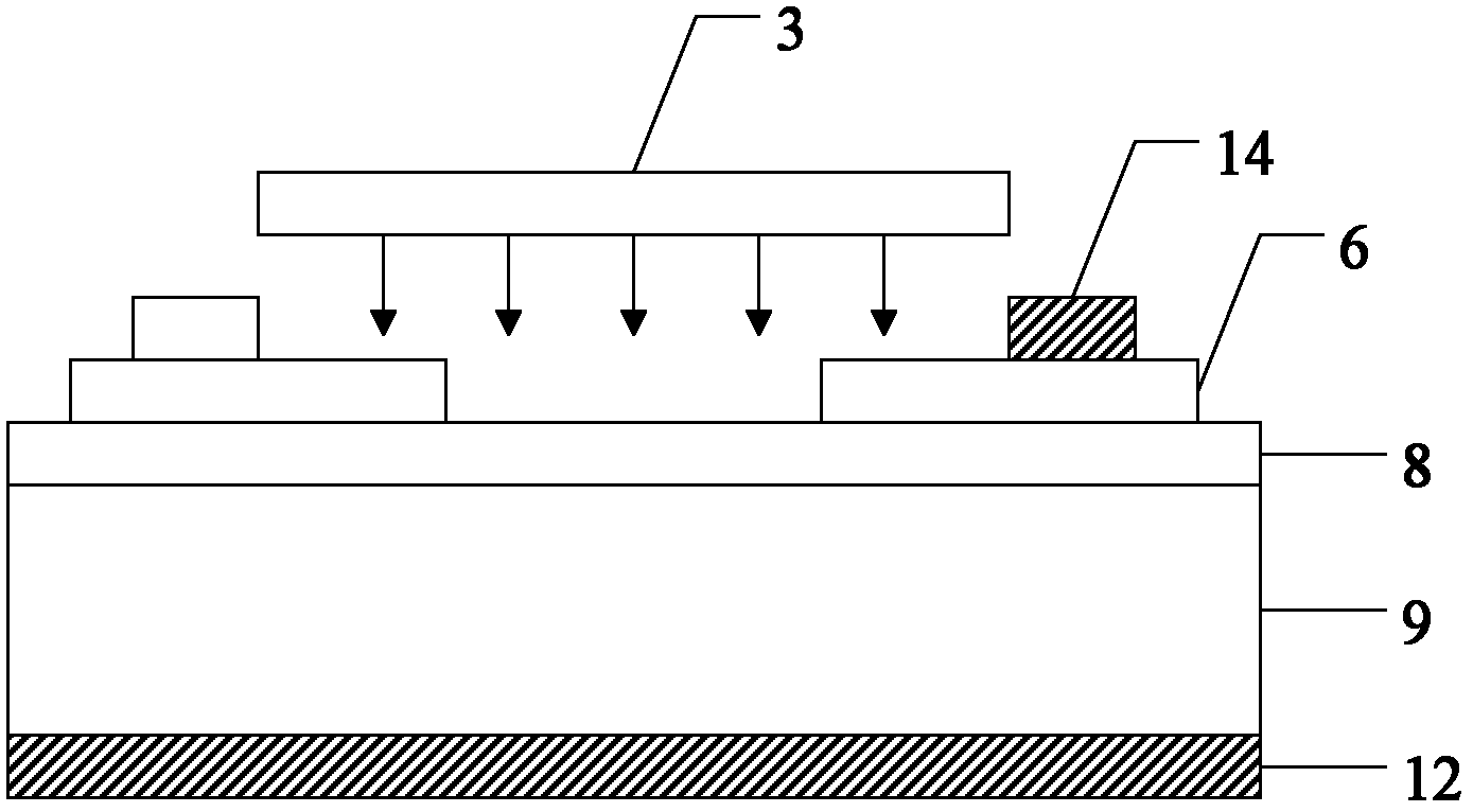
[0064] Step 3: Photolithography forms the mesa, such as Figure 6...

Embodiment 3

[0081] In step A, a low-doped n-type epitaxial layer is epitaxially grown on a SiC highly-doped n-type substrate sample, such as Figure 6 a.

[0082] The doping concentration will be selected as 7×10 18 cm -3 After cleaning the n-type highly doped SiC substrate sample 7, the epitaxial growth thickness is 5 μm, and the doping concentration is 5×10 15 cm -3 The n-type low nitrogen-doped ion epitaxial layer 6, the epitaxial growth process conditions are: the epitaxial temperature is 1570°C, the pressure is 100mbar, the reaction gas is silane and propane, the carrier gas is pure hydrogen, and the impurity source is liquid nitrogen.

[0083] Step B: Epitaxial growth of highly doped p-type epitaxial layer, such as Figure 6 b.

[0084] Under the condition that the epitaxial temperature is 1570°C, the pressure is 100mbar, the reaction gas is silane and propane, the carrier gas is pure hydrogen, and the impurity source is trimethylaluminum, epitaxially grow aluminum ion-doped ep...


PUM

PropertyMeasurementUnit
thicknessaaaaaaaaaa
thicknessaaaaaaaaaa
thicknessaaaaaaaaaa

Abstract

The invention discloses a silicon carbide gridding electrode PIN type nuclear battery and a manufacturing method thereof. By the silicon carbide gridding electrode PIN type nuclear battery and the manufacturing method thereof, the problem of low conversion efficiency during the manufacturing of silicon carbide PIN nucleus batteries in the prior art is solved. The silicon carbide gridding electrode PIN type nuclear battery comprises a radioactive isotope source layer (1), a SiO2 compact insulating layer (2), a SiO2 passivation layer (3), a p type ohmic contact electrode (4), a p type SiC epitaxial layer (5) of which the doping density is between 1*10<19> and 5*10<19>cm<-3>, an n type SiC epitaxial layer (6) of which the doping density is between 1*10<15> and 5*10<15>cm<-3>, an n type SiC substrate (7) of which the doping density is between 1*10<18> and 7*10<18>cm<-3> and an n type ohmic contact electrode (8), wherein the p type ohmic contact electrode (4) consists of a plurality of identical square grids, the square grids are formed by partitioning a plurality of transverse rectangular strips and a plurality of longitudinal rectangular strips, and a plurality of pins are reserved at the periphery of the integral grid electrode; and the radioactive isotope source layer (1) covers the surface of the p type ohmic contact electrode (4). The silicon carbide gridding electrode PIN type nuclear battery is high in energy conversion efficiency, and can be used as micro-electromechanical system (MEMS) on-chip power supplies, cardiac pacemaker power supplies and mobile standby power supplies.

Description

technical field [0001] The invention belongs to the field of microelectronics, and in particular relates to a PIN type nuclear battery based on silicon carbide grid electrodes, which can be used to directly convert nuclear energy emitted by isotopes into electric energy. technical background [0002] In 1953, Rappaport discovered that the beta (β-Particle) particles produced by the decay of isotopes can generate electron-hole pairs in semiconductors. This phenomenon is called β-Voltaic Effect. Shortly thereafter, Elgin-Kidde first used the β-Voltaic Effect in power supply in 1957, and successfully manufactured the first isotope micro-battery β-Voltaic Battery. Since 1989, GaN, GaP, AlGaAs, polysilicon and other materials have been used as materials for β-Voltaic batteries. With the preparation of the wide bandgap semiconductor material SiC and the advancement of process technology, since 2006, there have been reports on SiC-based isotope micro-batteries at home and abroad. ...

Claims


Application Information

Patent Timeline
Patent Type & Authority Applications(China)
IPC IPC(8): G21H1/06
Inventor 郭辉张玉娟张玉明石彦强项萍
Owner XIDIAN UNIV
Why Eureka
Try Eureka