Device and method for laser etching OLED display anode thin film material

A technology of laser etching and anode film, which is applied in laser welding equipment, welding equipment, metal processing equipment, etc., can solve the problems of complex and cumbersome procedures, difficult spacing control, and weak selectivity, and achieve good etching linearity, High luminous efficiency and fine line width

Inactive Publication Date: 2011-12-21
SUZHOU DELPHI LASER
View PDF7 Cites 14 Cited by
  • Summary
  • Abstract
  • Description
  • Claims
  • Application Information

AI Technical Summary

Problems solved by technology

[0005] The purpose of the present invention is to overcome the deficiencies in the prior art, to provide a device and method for laser etching the anode film material of OLED display, to realize etching the anode of OLED display, to obtain thinner and more stable line width, and not Damage the substrate, so as to overcome the shortcomings of traditional chemical wet etching methods such as complex and cumbersome procedures, difficult spacing control, poor selectivity, and environmental pollution

Method used


Image

  • Device and method for laser etching OLED display anode thin film material
  • Device and method for laser etching OLED display anode thin film material
  • Device and method for laser etching OLED display anode thin film material

Examples


Embodiment Construction

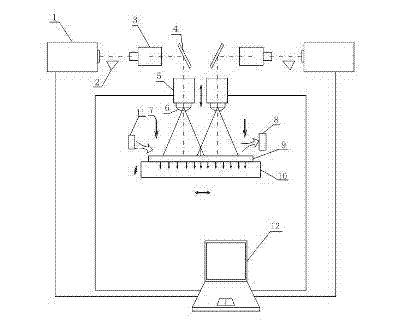
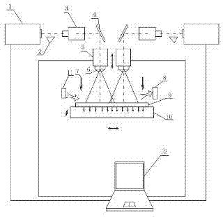
[0015] The present invention proposes a micromachining method and system for applying laser etching to the anode of OLED displays. Laser etching can avoid the inherent disadvantages of chemical wet methods, and the laser has the characteristics of non-contact, non-polluting environment, and easy control, making it an OLED display An important application hotspot of anode pattern line width control, and will gradually be widely used in industry. The use of lasers to etch the anode of OLED displays can achieve a relatively stable line width, making the line width of the anode as thin as 20um. During production, the etched pattern can be easily replaced without waste generation, which can save a lot of research and development costs and shorten the product development cycle. The high-precision control system can perform high-efficiency etching, which is fast, stable, and highly repeatable. It can ensure the stability and precision of processing and greatly improve the yield rate. ...


PUM

PropertyMeasurementUnit
wavelengthaaaaaaaaaa

Abstract

The invention relates to a device and a method for laser etching the anode film material of an OLED display. The output end of the high-frequency short-pulse laser is arranged with an electric shutter, the output end of the electric shutter is provided with an electric beam expander, and the output end of the electric beam expander A 45-degree total reflection mirror is arranged in sequence, and the output end of the 45-degree total reflection mirror is arranged with a vibrating mirror and a scanning field mirror. The scanning field mirror is facing the three-axis adsorption platform, and one side of the three-axis adsorption platform is equipped with an ion wind blower system, the dust collection system is installed on the other side, the CCD alignment observation system is installed at the diagonal positions on the three-axis adsorption platform, and the high-frequency short-pulse laser and the vibrating mirror are connected to the industrial computer. Using high-frequency pulsed lasers of different wavelengths as the laser source, laser etching is performed on the anode material of the OLED display, so that the anode material of the OLED display is vaporized under the action of the high-frequency short-pulse laser to achieve the purpose of erosion, and the processed product is pollution-free. , OLED display products with stable linearity and good functions.

Description

technical field [0001] The invention relates to a micro-machining method and equipment for using a laser to etch an anode film material of an OLED display. Background technique [0002] In recent years, organic light emitting diode (OLED) has become a very popular emerging flat panel display industry, mainly because OLED displays have self-illumination, wide viewing angle (over 170 degrees), and fast response time (on the order of 1 μs). , high luminous efficiency, low working voltage (3-10V), thin panel thickness (less than 2mm), large-size and bendable (flexible) panels can be produced, the process is simple, and it has low-cost potential (expected to be lower than TFT- LCDs are about 20% cheaper). [0003] The OLED device structure can be roughly divided into four main areas: substrate, cathode, organic light-emitting material and anode. In order to effectively inject electrons or holes into organic materials, as mentioned above, lowering the injection energy barrier i...

Claims


Application Information

Patent Timeline
Patent Type & Authority Applications(China)
IPC IPC(8): B23K26/36B23K26/14B23K26/362
Inventor 赵裕兴狄建科张伟
Owner SUZHOU DELPHI LASER
Why Eureka
Try Eureka