Silicon detector structure with broad spectral response and method of making same

A wide spectrum and detector technology, applied in the field of silicon detector structure and fabrication, can solve the problems of serious Auger recombination in heavily doped surface layer, low mobility of black silicon material, high infrared light transmittance, etc. Response range, counteracting low mobility, counteracting effect of short carrier lifetime

Inactive Publication Date: 2011-12-21
INST OF SEMICONDUCTORS - CHINESE ACAD OF SCI
View PDF3 Cites 30 Cited by
  • Summary
  • Abstract
  • Description
  • Claims
  • Application Information

AI Technical Summary

Problems solved by technology

[0004] In 2005, they used black silicon material as the photosensitive area of ​​the light-facing surface of the detector, and achieved a certain infrared responsivity in two important optical fiber windows of 1330nm and 1550nm [Opt.Lett.30, 1773-1775(2005)], but Due to the low mobility of black silicon materials, short carrier lifetime, serious Auger recombination on the heavily doped surface layer, and large infrared light transmittance, the further improvement of the infrared spectral responsivity of black silicon detectors is restricted.

Method used


Image

  • Silicon detector structure with broad spectral response and method of making same
  • Silicon detector structure with broad spectral response and method of making same
  • Silicon detector structure with broad spectral response and method of making same

Examples


Embodiment Construction

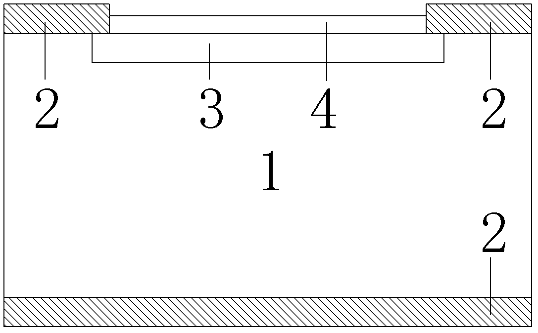
[0031] see Figure 1g , the present invention provides a silicon detector structure with wide spectral response, the structure includes from top to bottom:

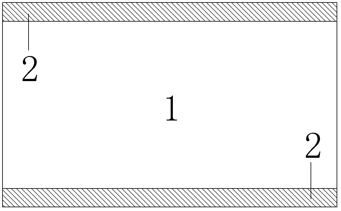
[0032] An n-type silicon-based substrate layer 1 with a circular groove on the surface; the n-type silicon-based substrate layer 1 is made of n-type (111) single crystal silicon, with a thickness of 100 to 500 μm and a resistivity of 1 to 1000 Ω·cm;

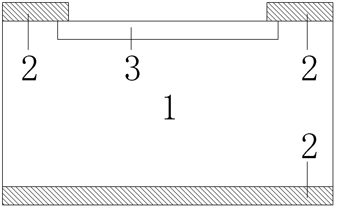
[0033] A silicon dioxide dielectric masking layer 2, formed on the periphery of the circular groove on the surface of the n-type silicon-based substrate layer 1, with a ring structure in the middle;

[0034] A p-type doped layer 3 is located in the circular groove of the n-type silicon-based substrate layer 1; the p-type doped layer 3 is formed by boron ion implantation or boron diffusion on the surface of the n-type silicon-based substrate layer 1 , the p-type doped layer 3 forms a pn junction photosensitive region with the n-type silicon-based substrate layer 1;

[0035]...


PUM


Abstract

The invention relates to a silicon detector structure with a wide spectral response range, which comprises an n-type silicon substrate, a silicon dioxide medium masking layer, a p-type doping layer, a front surface contact electrode, an antireflection film layer, a broad-spectrum absorbing black silicon layer, a medium passivating layer and a back surface contact electrode, wherein a circular groove is arranged on the surface of the n-type silicon substrate; the silicon dioxide medium masking layer is formed around the circular groove on the surface of the n-type silicon substrate, and the middle of the silicon dioxide medium masking layer is an annular structure; the p-type doping layer is arranged in the circular groove of the n-type silicon substrate; the front surface contact electrode is produced on the inner wall of the annular structure of the silicon dioxide medium masking layer and covers the partial edge of the surface of the annular structure to form an annular structure; the antireflection film layer is produced in the annular structure of the front surface contact electrode and covers the surface of the p-type doping layer; the broad-spectrum absorbing black silicon layer is produced on the back surface of the n-type silicon substrate; the medium passivating layer is point-type and is formed on the surface of the broad-spectrum absorbing black silicon layer; and the back surface contact electrode is produced on the surface of the broad-spectrum absorbing black silicon layer and covers the point-type medium passivating layer.

Description

technical field [0001] The invention relates to a photodetector structure and a manufacturing method thereof, in particular to a silicon detector structure with wide spectral response and a manufacturing method thereof. Background technique [0002] For ordinary crystalline silicon, on the one hand, due to its forbidden band width of 1.12ev, it cannot absorb light with a wavelength greater than 1.1 μm, which limits the usable band and sensitivity of silicon optoelectronic devices; on the other hand, although it is made of ordinary crystalline silicon p-n and p-i-n photodetectors have been realized for a long time, but the peak response of this kind of detector is about 900nm, which is only suitable for the detection of 850nm band, and cannot be applied to the two important optical fiber communication windows of 1310nm and 1550nm. Although the technology of III-V materials has matured and achieved industrialization in this area, they are expensive, have poor thermal and mecha...

Claims


Application Information

Patent Timeline
Patent Type & Authority Applications(China)
IPC IPC(8): H01L31/101H01L31/028H01L31/0352H01L31/18
CPCY02P70/50
Inventor 刘德伟黄永光朱小宁王熙元马丽朱洪亮
Owner INST OF SEMICONDUCTORS - CHINESE ACAD OF SCI
Why Eureka
Try Eureka