Preparation method of Al-doped zinc oxide transparent conductive thin film

A transparent conductive thin film, chemical formula technology, applied in metal material coating process, vacuum evaporation coating, coating and other directions, can solve the problem of large area uniform coating, high temperature of thin film deposition substrate, large difference in conductivity, etc. problems, to achieve the effect of low cost, dense crystals, improved uniformity and compactness

Active Publication Date: 2012-01-11
SHANGHAI INST OF CERAMIC CHEM & TECH CHINESE ACAD OF SCI
View PDF6 Cites 9 Cited by
  • Summary
  • Abstract
  • Description
  • Claims
  • Application Information

AI Technical Summary

Problems solved by technology

Although PLD and MBE can prepare high-quality films, they are not conducive to large-scale applications; films prepared by sputtering or evaporation usually have poor surface quality, high roughness, and large differences in conductivity; USP and Sol-Gel belong to chemical preparation, the film quality is relatively low, and it is not conducive to large-scale production
Except for the chemical vapor deposition (CVD) method, other methods have not reached the level of large-area uniform coating (industrial production), but the main disadvantage of the CVD method is that the equipment is complex and expensive, and the organic zinc source used is expensive and toxic. High substrate temperature

Method used


Image

  • Preparation method of Al-doped zinc oxide transparent conductive thin film
  • Preparation method of Al-doped zinc oxide transparent conductive thin film
  • Preparation method of Al-doped zinc oxide transparent conductive thin film

Examples


Embodiment 1

[0035] Doped ZnO thin film Zn with 2 mol% Al 0.98 al 0.02 O as an example:

[0036] (1) Zn was prepared by a standard isostatic solid-state reaction synthesis process 0.98 al 0.02 O target. Press Zn with electronic balance 0.98 al 0.02 The stoichiometric ratio of the corresponding elements of O Weigh high-purity (≥99.99%) ZnO (40.695g) and Al 2 o 3 (0.520g), after being fully mixed, pre-pressed (50MPa), then cold isostatic pressed (200MPa), and finally placed in a tubular electric furnace and gradually heated to 1000 ° C, and kept for 48 hours.

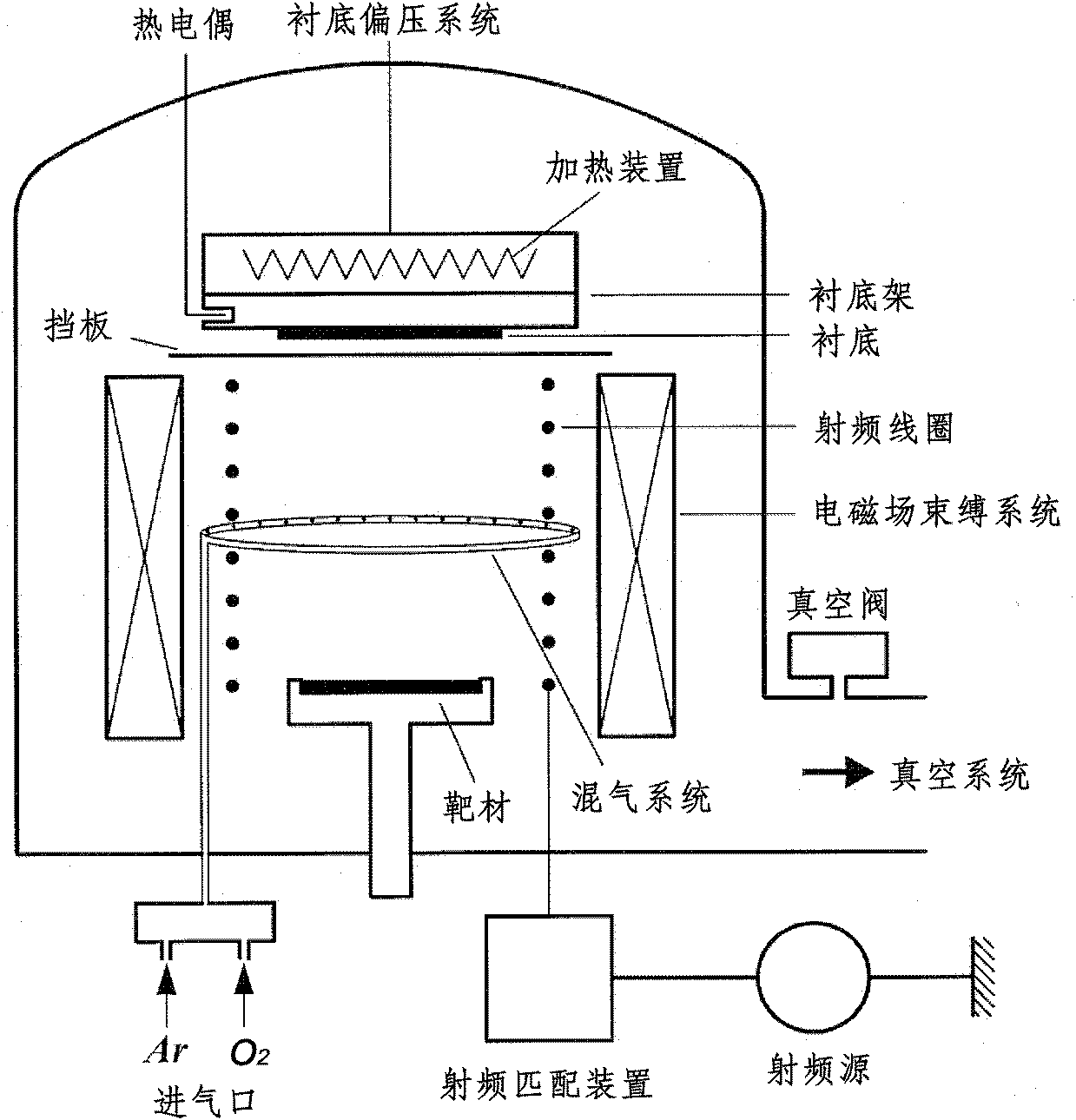
[0037] (2) The quartz glass substrate is cleaned with N 2 Blow dry and place in the ICP-PVD reaction chamber.

[0038] (3) Pump the background vacuum of the ICP-PVD system to 1×10 -7 Torr, and then heat the substrate, the substrate temperature is 400°C.

[0039] (4) Using high-purity (≥99.9995%) Ar as the carrier gas and plasma source, the reaction chamber pressure is 100 Torr, the RF sputtering power is 150W, the binding c...

Embodiment 2

[0048] ZnO thin film doped with 1% Al by mole Zn 0.99 al 0.01 O as an example:

[0049] (1) Zn was prepared by a standard isostatic solid-state reaction synthesis process 0.99 al 0.01 O target. Press Zn with electronic balance 0.99 al 0.01 The stoichiometric ratio of the corresponding elements of O Weigh high-purity (≥99.99%) ZnO (40.695g) and Al 2 o 3 (0.257g), after being fully mixed, pre-pressed (50MPa), then cold isostatic pressed (200MPa), and finally placed in a tubular electric furnace and gradually heated to 1000 ° C, and kept for 48 hours.

[0050] (2) Clean the Si substrate with N 2 Blow dry and place in the ICP-PVD reaction chamber.

[0051] (3) Pump the background vacuum of the ICP-PVD system to 5×10 -8 Torr, and then heat the substrate, the substrate temperature is 300°C.

[0052] (4) Using high-purity (≥99.9995%) Ar as the carrier gas and plasma source, the reaction chamber pressure is 50Torr, the RF sputtering power is 200W, the binding coil current i...

Embodiment 3

[0057] Doped ZnO thin film Zn with 5 mol% Al 0.95 al 0.05 O as an example:

[0058] (1) Zn was prepared by a standard isostatic solid-state reaction synthesis process 0.95 al 0.05 O target. Press Zn with electronic balance 0.95 al 0.05 The stoichiometric ratio of the corresponding elements of O Weigh high-purity (≥99.99%) ZnO (40.695g) and Al 2 o 3 (1.342g), after being fully mixed, pre-pressed (50MPa), then cold isostatic pressed (200MPa), and finally placed in a tubular electric furnace and gradually heated to 1000 ° C, and kept for 48 hours.

[0059] (2) Clean the Si substrate with N 2 Blow dry and place in the ICP-PVD reaction chamber.

[0060] (3) Pump the background vacuum of the ICP-PVD system to 5×10 -8 Torr, and then heat the substrate, the substrate temperature is 350°C.

[0061] (4) Use high-purity (≥99.9995%) Ar as the carrier gas and plasma source, the reaction chamber pressure is 50Torr, the RF sputtering power is 150W, the binding coil current is 0.4 ...


PUM

PropertyMeasurementUnit
mean roughnessaaaaaaaaaa
surface roughnessaaaaaaaaaa

Abstract

The invention belongs to the field of transparent conductive thin films, relates to a preparation method of an Al-doped ZnO transparent conductive thin film, and in particular relates to an inductively coupled plasma reinforced physical vapour deposition (ICP-PVD) method. The ICP-PVD method comprises the following steps of: firstly preparing a Zn1-xAlxO (x is more than or equal to 0.01 and is less than or equal to 0.05) target material; and placing a clean and dry substrate into an ICP-PVD system, and controlling all the technological parameters of the ICP-PVD system to carry out thin film deposition, so as to obtain the Al-doped ZnO transparent conductive thin film. The method provided by the invention adopts simple equipment, is easy to operate and can realize large-area and mass production of coating films. Compared with the traditional thin film equipment, the ICP-PVD system realizes constrain and acceleration effects on various charged particles in plasma, thus crystallization quality of the thin film and controllability of doping of a donor are improved, a ZnO thin film with low resistivity, high transmissivity and good repeatability and stability can be easily obtained, andthe thin film can be applied to photoelectronic devices.

Description

technical field [0001] The invention belongs to the field of transparent conductive films, and relates to a method for preparing an Al-doped zinc oxide transparent conductive film, in particular to an inductively coupled plasma enhanced physical vapor deposition method. Background technique [0002] Transparent conductive film technology began in the early 20th century. With the development of electronic technology, it has been widely used in flat-panel displays, transparent heating components, antistatic films, electromagnetic wave protective films, transparent electrodes of solar cells, anti-reflective coatings and heat sinks since the 1990s. Mirrors and other optical, electronic and optoelectronic devices. In the field of flat panel display, liquid crystal display has become the leading product in the present and future market, and its market output value will grow geometrically. It is estimated that the global overall liquid crystal display industry output value will rea...

Claims


Application Information

Patent Timeline
Patent Type & Authority Applications(China)
IPC IPC(8): C23C14/34C23C14/08
Inventor 刘学超陈之战宋力昕施尔畏
Owner SHANGHAI INST OF CERAMIC CHEM & TECH CHINESE ACAD OF SCI
Why Eureka
Try Eureka