Preparation method of vertical silicon nanowire field effect transistor

A field-effect transistor and silicon nanowire technology, which is applied in nanotechnology, nanotechnology, semiconductor/solid-state device manufacturing, etc., can solve the problems of vertical silicon nanowire field-effect transistors, such as difficult source-drain and gate self-alignment

Active Publication Date: 2012-01-11
SEMICONDUCTOR MANUFACTURING INTERNATIONAL (BEIJING) CORP +1
View PDF5 Cites 8 Cited by
  • Summary
  • Abstract
  • Description
  • Claims
  • Application Information

AI Technical Summary

Problems solved by technology

On the other hand, the difficulty in realizing the vertical silicon nanowire field effect transistor lies in the self-alignment of the source, drain and gate.

Method used


Image

  • Preparation method of vertical silicon nanowire field effect transistor
  • Preparation method of vertical silicon nanowire field effect transistor
  • Preparation method of vertical silicon nanowire field effect transistor

Examples


Embodiment Construction

[0099] The present invention will be described in detail below in conjunction with the accompanying drawings and specific embodiments, and a process scheme for implementing a vertical silicon nanowire field-effect transistor with a small parasitic resistance proposed by the present invention is specifically provided, but the scope of the present invention is not limited in any way. scope.

[0100] A vertical silicon nanowire field effect transistor with a channel length of about 90 nanometers and a diameter of about 10 nanometers was prepared according to the following steps:

[0101] 1. Low pressure chemical vapor deposition silicon oxide 300

[0102] 2. Low pressure chemical vapor deposition silicon nitride 1000

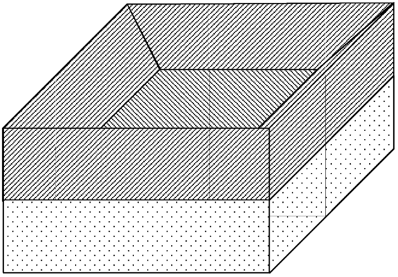
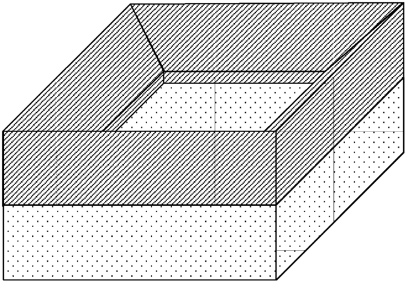
[0103] 3. Optical lithography to define the active area;

[0104] 4. Anisotropic dry etching 1000 silicon nitride;

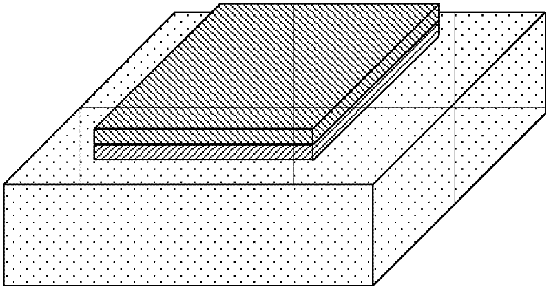
[0105] 5. BHF solution corrosion 300 Silicon oxide, overetched for 5s, such as Figure 1A shown;

[0106] 6. Remove the photoresist;

...


PUM


Abstract

The invention, which belongs to the super-large-scale integrated circuit manufacturing technology field, provides a preparation method of a vertical silicon nanowire field effect transistor with a small parasitic resistance. Compared to a traditional plane field effect transistor, by using the vertical silicon nanowire field effect transistor prepared in the invention, on one hand, a good abilityof restraining a short channel effect can be provided and leakage current and drain induced barrier lowering (DIBL) can be reduced because of a good gate control ability caused by a one-dimensional geometric structure of the vertical silicon nanowire field effect transistor; on the other hand, a device area can be further reduced and an integration level of an IC system can be raised.

Description

technical field [0001] The invention relates to a preparation method of a vertical silicon nanowire field effect transistor with small parasitic resistance, and belongs to the technical field of VLSI manufacturing. Background technique [0002] As the fastest-growing science and technology in the 20th century, semiconductor manufacturing technology is gradually covering the entire industrial production network, and semiconductor technology is playing a huge role everywhere in life. While people are pursuing the excellent performance of semiconductor electronic products such as mobile phones and computers, they also do not forget to make them smaller in size, smaller in space, and easier to carry and operate. Therefore, under the guidance of Moore's Law, the entire semiconductor industry regards integration, low power consumption, and high performance as the goals of advancement. With the continuous reduction of feature size, how to deal with the increasingly serious short c...

Claims


Application Information

Patent Timeline
Patent Type & Authority Applications(China)
IPC IPC(8): H01L21/336B82Y40/00B82Y10/00
CPCH01L29/66772H01L29/78642B82Y40/00H01L29/0676H01L29/42392B82Y10/00H01L29/78696
Inventor 黄如樊捷闻艾玉杰孙帅王润声邹积彬黄欣
Owner SEMICONDUCTOR MANUFACTURING INTERNATIONAL (BEIJING) CORP
Why Eureka
Try Eureka