Solar panel preparing method

A technology of solar cells and silicon wafers, applied in circuits, electrical components, photovoltaic power generation, etc., can solve problems affecting the photoelectric conversion efficiency of solar cells, many impurities and micro-defects in solar cells, and carrier recombination

Active Publication Date: 2012-01-11
BYD CO LTD
View PDF5 Cites 5 Cited by
  • Summary
  • Abstract
  • Description
  • Claims
  • Application Information

AI Technical Summary

Problems solved by technology

[0006] In order to solve the problem that there are still many impurities and micro-defects in the solar cells prepared by the prior art, which easily cause carrier recombination and affect the photoelectric conversion efficiency of solar cells, the present invention provides a method that can significantly reduce the impurities in silicon chips. Method for preparing solar cells with micro-defects

Method used


Image

  • Solar panel preparing method
  • Solar panel preparing method
  • Solar panel preparing method

Examples


preparation example Construction

[0015] The invention provides a method for preparing a solar cell, the steps comprising:

[0016] a, preparing a-Si:H thin film on the surface of the silicon wafer after texturing;

[0017] b. Treating the silicon wafer containing the a-Si:H film on the surface obtained in step a at a high temperature of 800-900° C. for 60-120 min;

[0018] c. Etching the surface of the high temperature treated silicon wafer.

[0019] It can be combined with phosphorus diffusion treatment, and the front side of the silicon wafer deposited with a-Si:H film can be treated with phosphorus diffusion at the same time of high temperature treatment. In this case, the thickness of the a-Si:H film deposited on the back and front of the silicon wafer Different, the thickness of the a-Si:H film deposited on the front side is generally thinner, which is made into an oxide layer, and then phosphorus diffusion treatment is performed to prepare a perfect PN junction. It is preferable to remove the gettered...

Embodiment 1

[0030] Gettering and Diffusion Processes in the Preparation of Solar Cells

[0031] a) Using plasma enhanced chemical vapor deposition (PECVD), SiH 4 and H 2 For the reaction gas, SiH 4 and H 2 Plasma occurs under the action of microwaves, and then reacts to form a-Si:H film on the back surface of the textured silicon wafer. The substrate temperature is 400°C, the microwave power is 3000W, the power frequency is 2.45GHz, and the reaction gas SiH 4 :H 2 =1:10, the deposition time is 200s, and the thickness of a-Si:H film is: 100nm.

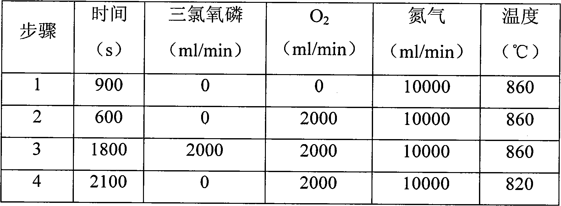
[0032] b) Insert the above-mentioned crystalline silicon wafers with a-Si:H thin film back-to-back into a quartz boat, and put them into a diffusion furnace (TS81254 model produced by Tempress Company) to carry out phosphorus diffusion and gettering, the time and temperature of each step of the process And the amount of each gas flow is shown in the table below:

[0033]

[0034] c) Use the back chemical etching to make the silicon wafer ...

Embodiment 2

[0036] Gettering and Diffusion Processes in the Preparation of Solar Cells

[0037] a) Using plasma enhanced chemical vapor deposition (PECVD), SiH4 and H 2 For the reaction gas, SiH 4 and H 2 Plasma occurs under the action of microwaves, and then reacts to form a-Si:H film on the back surface of the textured silicon wafer. The substrate temperature is 400°C, the microwave power is 3000W, the power frequency is 2.45GHz, and the reaction gas SiH 4 :H 2 =1:10, the deposition time is 200s, and the thickness of a-Si:H film is: 100nm.

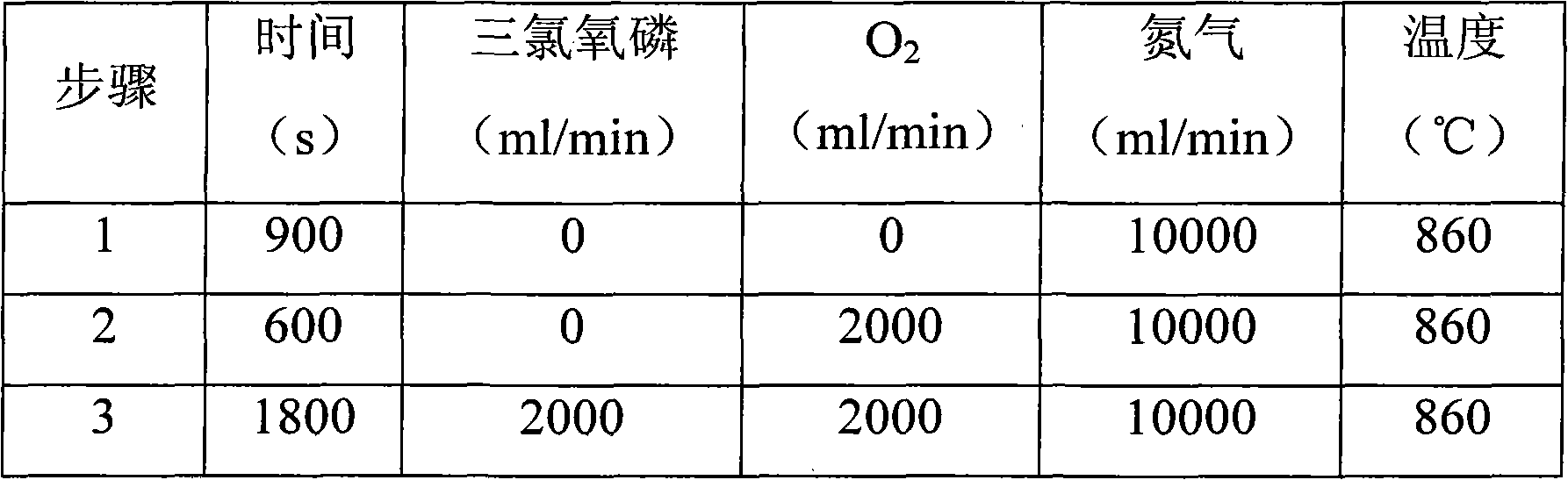
[0038] b) Put the crystalline silicon wafer with the a-Si:H thin film deposited on the backside into a high-temperature furnace and process at 860° C. for 90 minutes.

[0039] Finally, put the crystalline silicon wafer with the a-Si:H thin film deposited on the back after the high temperature treatment into the diffusion furnace for phosphorus diffusion process. The time, temperature and the amount of various gases in each step of this process ...


PUM

PropertyMeasurementUnit
thicknessaaaaaaaaaa
thicknessaaaaaaaaaa

Abstract

The invention provides a solar panel preparing method, which comprises the steps of: a, preparing a-Si:H film on the surface of a silicon chip after texturing; b, treating the silicon chip containing the a-Si:H film on the surface obtained in the step a at 800 to 900 DEG C for 60 to 120 min; and c, carrying out corrosion treatment on the surface of the silicon chip treated through high temperature. The solar panel preparing method has the advantages that a layer of a-Si:H film is deposited on the back surface of the silicon chip after the texturing, the problems of many impurities and micro defects in the silicon chip can be perfectly solved, the electrochemical performance such as the service life, the photoelectric conversion efficiency and the like of solar panels is improved, in addition, good back side and body passivation effects can be realized, the current and voltage (I-V) character of solar batteries is improved, and simultaneously, the process is simple and is easy to implement.

Description

technical field [0001] The invention relates to a method for preparing a solar battery sheet. Background technique [0002] With the depletion of traditional energy sources and the aggravation of environmental pollution, the development and application of new energy sources has become a hot spot in human research. Inexhaustible, green and pollution-free solar energy is one of the key points in the development and utilization of new energy. [0003] Silicon wafers are the core components of solar energy solar cells. Silicon wafers are generally made into silicon wafers after multi-step purification of raw silicon. Afterwards, silicon wafers undergo degreasing process→removal of damaged layer→texturing→diffusion process→peripheral engraving Etching→removing the oxide layer→making silicon nitride film→screen printing the back and positive electrode→sintering→testing and sorting to make solar cells. [0004] Solar cells have high requirements on the purity of silicon, generall...

Claims


Application Information

Patent Timeline
Patent Type & Authority Applications(China)
IPC IPC(8): H01L31/18H01L31/04
CPCY02E10/50Y02P70/50
Inventor 李燕燕
Owner BYD CO LTD
Why Eureka
Try Eureka