Silicon slice thinning method based on metal nano particle catalysis

A technology of metal nanoparticles and silicon wafers, which is applied in the field of microelectronics to achieve the effect of smooth silicon surface, simple operation and good repeatability

Active Publication Date: 2012-02-15
NORTH CHINA ELECTRIC POWER UNIV (BAODING)
View PDF4 Cites 11 Cited by
  • Summary
  • Abstract
  • Description
  • Claims
  • Application Information

AI Technical Summary

Problems solved by technology

However, there is no related report on the uniform corrosion of silicon surface by metal nanoparticle catalyzed etching method.

Method used


Image

  • Silicon slice thinning method based on metal nano particle catalysis
  • Silicon slice thinning method based on metal nano particle catalysis

Examples


Embodiment 1

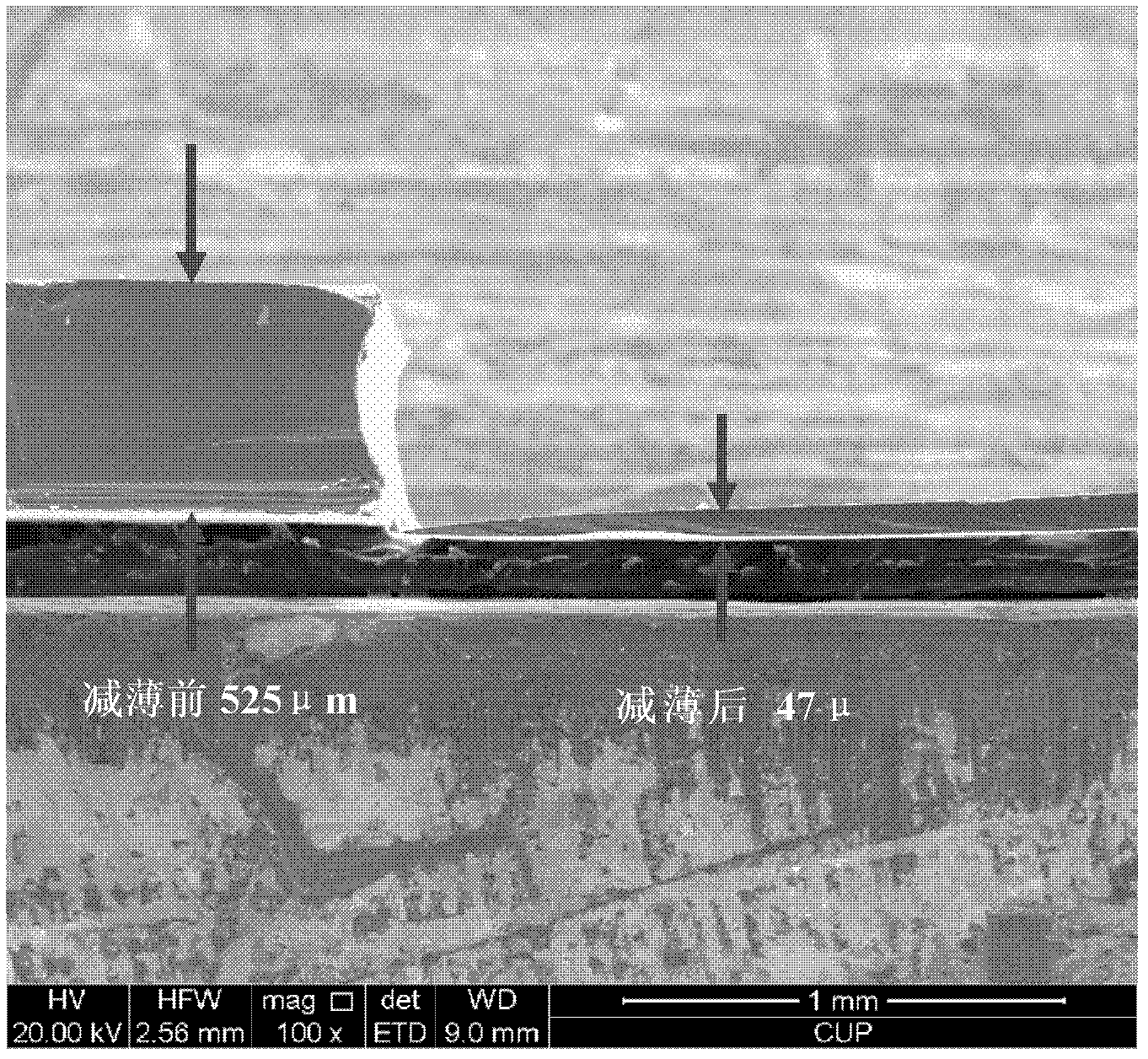
[0035] 1. Use a (100) monocrystalline silicon wafer with a resistivity of 7-13Ω·cm, with a thickness of 525 μm, ultrasonically clean it in acetone for 10 minutes; rinse it twice with deionized water, and then wash it in CP-4A solution Soak at room temperature for 5 minutes; then soak in hydrofluoric acid with a concentration of 7.3mol / L for 5 minutes at room temperature; rinse with deionized water for 2 minutes, and dry in vacuum; the resistivity of the deionized water is above 16MΩ·cm.

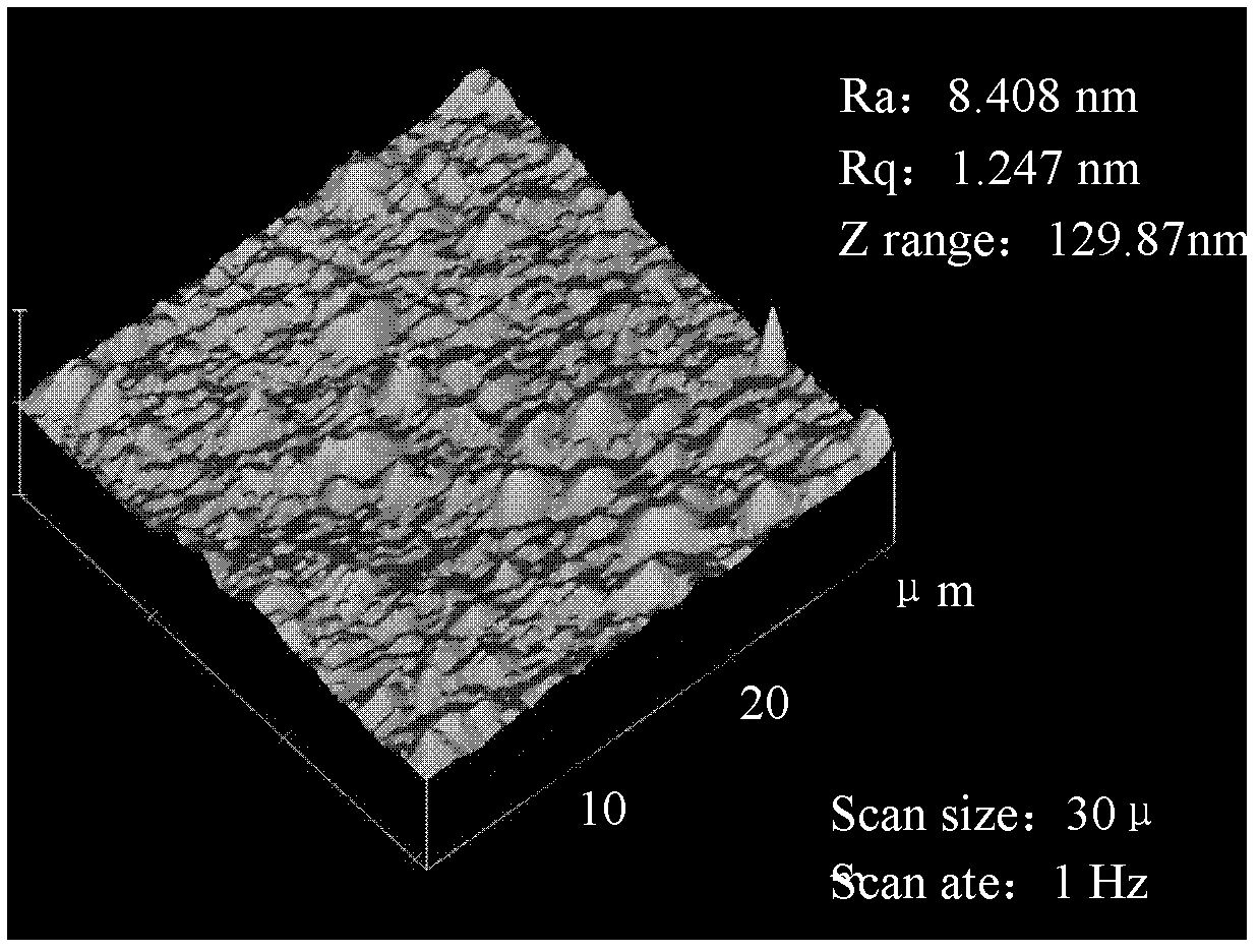
[0036]Described CP-4A solution is made of HF solution (mass fraction is 40%), HNO 3 solution, absolute ethanol, H 2 O is formulated at a volume ratio of 3:5:3:22, where HNO 3 The mass fraction of the solution is 68%, so as to ensure the polishing and etching of the silicon surface and the improvement of the surface quality.

[0037] 2. Use 40% (wt) HF solution, 30% (wt) hydrogen peroxide, deionized water (resistivity above 16MΩ·cm) and silver nitrate crystals to prepare a mixed solution wit...

Embodiment 2

[0044] Use a single crystal silicon wafer with a resistivity of 8-13Ω·cm and an orientation of (111), ultrasonically clean it in acetone for 10 minutes; rinse it twice with deionized water, and then soak it in CP-4A solution at room temperature for 5 minutes; Soak in 7.3mol / L hydrofluoric acid at room temperature for 5 minutes; rinse with deionized water for 2 minutes, and dry in vacuum;

[0045] Described CP-4A solution is made of HF solution (mass fraction is 40%), HNO 3 solution, absolute ethanol, H 2 O is formulated at a volume ratio of 3:5:3:22, where HNO 3 The mass fraction of the solution is 65%, so as to ensure the polishing and etching of the silicon surface and the improvement of the surface quality.

[0046] 2. Use 40% (wt) HF solution, 30% (wt) hydrogen peroxide, deionized water and silver nitrate crystals to prepare a mixed solution with the following concentration characteristics as the thinning solution: the concentration of silver nitrate is 0.01mol / L, and th...


PUM

PropertyMeasurementUnit
electrical resistivityaaaaaaaaaa

Abstract

The invention discloses a silicon slice thinning method based on metal nano particle catalysis in the technical field of microelectronics. The method comprises the following steps of: pretreating a silicon slice (100) or (111) at normal temperature by using acetone, a CP4-A solution and hydrofluoric acid so as to obtain a clean silicon surface; and preparing a thinning solution which is formed byuniformly mixing silver nitrate, hydrogen peroxide and hydrofluoric acid, putting the thinning solution into a water bath for preheating, immersing the silicon slice into the thinning solution, and thus obtaining an ultrathin silicon slice with a required thickness by controlling reaction time, temperature and a solution ratio. In the method, the silicon slice can be uniformly etched by using a metal nano particle catalysis characteristic at the first time; a silicon slice thinning process is simplified by using a one-step method; characteristics of wet etching at near normal temperature and normal pressure can be retained, so the ultrathin silicon slice with the thickness of less than 50 microns can be obtained; furthermore, an application range of metal nano particle catalysis silicon etching is expanded; and a new idea and a new technical measure can be supplied to the silicon slice thinning process.

Description

technical field [0001] The invention belongs to the technical field of microelectronics, and relates to a method for thinning a single crystal silicon wafer in the preparation of semiconductor devices. It specifically relates to the metal nanoparticle catalyzed uniform corrosion process technology of the silicon wafer thinning process. Background technique [0002] Silicon wafer thinning technology has high production efficiency and excellent thickness and dimension control characteristics, and was first applied to the treatment of silicon wafer cutting defects caused by inner circle slicing. With the rapid development of integrated circuit packaging technology, the miniaturization and intelligence of electronic terminal equipment put forward higher requirements for the improvement of chip packaging structure and heat dissipation efficiency. Ultra-thin chips (<50 μm) have become the main building blocks of micro-smart device stacking / 3D packaging, and the preparation of ...

Claims


Application Information

Patent Timeline
Patent Type & Authority Applications(China)
IPC IPC(8): H01L21/302
Inventor 李美成白帆任霄峰余航
Owner NORTH CHINA ELECTRIC POWER UNIV (BAODING)
Why Eureka
Try Eureka