Resistance-type gas sensor with two support suspension beams and four-layer structure and method

A gas sensor, resistive technology, applied in the field of micro-electronic mechanical systems and gas sensing, can solve the problems of strict environmental conditions, expensive process equipment, high power consumption, achieve high mechanical strength, reduce the number of thin film layers, and low cost. Effect

Inactive Publication Date: 2012-02-22
SHANGHAI INST OF MICROSYSTEM & INFORMATION TECH CHINESE ACAD OF SCI
View PDF4 Cites 13 Cited by
  • Summary
  • Abstract
  • Description
  • Claims
  • Application Information

AI Technical Summary

Problems solved by technology

Thin-film gas sensors have the advantages of low material consumption, repeatability between sensors, and good mechanical strength of the sensor, but the manufacturing process of thin-film sensors requires complex and expensive process equipment, strict environmental conditions, and high cost
The silicon-based microstructure thin-film gas sensor is a new type of resistive gas sensor based on a micro-heater. The current mainstream is based on a closed-membrane or four-cantilever-beam micro-heater, and the power consumption is relatively high.

Method used


Image

  • Resistance-type gas sensor with two support suspension beams and four-layer structure and method
  • Resistance-type gas sensor with two support suspension beams and four-layer structure and method
  • Resistance-type gas sensor with two support suspension beams and four-layer structure and method

Examples


Embodiment 1

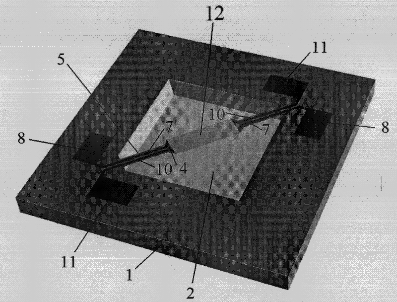
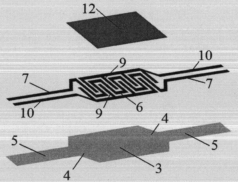
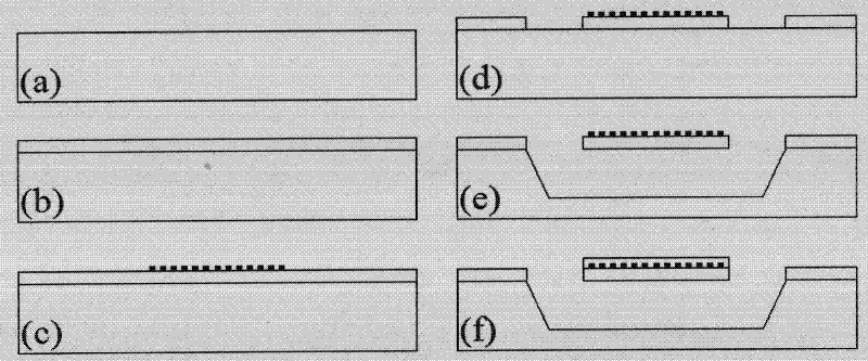
[0037] The structure schematic diagram of this embodiment sees figure 1 As shown, the specific production method is as follows:

[0038] 1. Select the substrate. A 4-inch double-sided polished silicon wafer with an N-type (100) surface is selected as a substrate, the resistivity is 3-8Ω·cm, the thickness of the silicon wafer is 350±10 microns, and the angle error of trimming is <1%.

[0039] 2. Make a composite film. A single-layer composite film is used to sequentially grow a layer of silicon oxide with a thickness of 0.5 microns and a layer of silicon nitride with a thickness of 0.3 microns by means of low-pressure chemical vapor deposition (LPCVD).

[0040] 3. Make heating resistance wire, power supply lead, power supply electrode, interdigital electrode, detection lead and detection electrode. Manufactured using a lift-off process. Thin resist lithography (photoresist thickness is 2.0 microns) defines the pattern of heating resistance wire, power supply lead, power sup...

Embodiment 2

[0045] The structure schematic diagram of this embodiment sees Figure 4 As shown, the specific production method is as follows:

[0046] 1. Select the substrate. A 4-inch double-sided polished silicon wafer with a P-type (100) surface is selected as the substrate, the resistivity is 3-8Ω·cm, the thickness of the silicon wafer is 350±10 microns, and the angle error of the edge trimming is less than 1%.

[0047] 2. Make a composite film. Using a single-layer composite film, a layer of silicon oxide with a thickness of 0.4 microns and a layer of silicon nitride with a thickness of 0.6 microns are sequentially grown by plasma enhanced chemical vapor deposition (PECVD).

[0048] 3. Make heating resistance wire, power supply lead, power supply electrode, interdigital electrode, detection lead and detection electrode. Manufactured by lift-off process. Thin photolithography (photoresist thickness is 2.0 microns) defines the pattern of heating resistance wire, power supply lead, p...

Embodiment 3

[0053] The structure schematic diagram of this embodiment sees Figure 5 As shown, the specific production method is as follows:

[0054] 1. Select the substrate. A 4-inch double-sided polished silicon wafer with a P-type (111) surface is selected as the substrate, the resistivity is 3-8Ω·cm, the thickness of the silicon wafer is 350±10 microns, and the angle error of the edge trimming is less than 1%.

[0055] 2. Make a composite film. Using a multi-layer composite film, a layer of silicon oxide with a thickness of 0.2 microns and a layer of silicon nitride with a thickness of 0.2 microns are sequentially deposited by low-pressure chemical vapor deposition (LPCVD), and then plasma-enhanced chemical vapor deposition (PECVD) A method of depositing a layer of silicon oxide with a thickness of 0.2 microns and a layer of silicon nitride with a thickness of 0.2 microns in sequence.

[0056] 3. Make heating resistance wire, power supply lead, power supply electrode, interdigital ...


PUM

PropertyMeasurementUnit
electrical resistivityaaaaaaaaaa
thicknessaaaaaaaaaa

Abstract

The invention relates to a resistance-type gas sensor with two support suspension beams and a four-layer structure and a manufacturing method for the sensor. The sensor comprises a substrate frame, a heat insulation cavity, a heating membrane area, a transition area, the support suspension beams, a heating resistance wire, a power supply lead, a power supply electrode, interdigital electrodes, a detection lead, a detection electrode and a sensitive membrane. The resistance-type gas sensor is characterized in that: the heating membrane area positioned above the heat insulation cavity is connected with the substrate frame by the transition area and the support suspension beams; the heating resistance wire is arranged on the heating membrane area in a mode of a crease line and is connected with the power supply electrode on the substrate frame through the power supply lead; the interdigital electrodes are arranged in a gap of the heating resistance wire and are connected with the detection electrode by the detection lead; and the sensitive membrane is positioned on the heating membrane area to cover the integral heating resistance wire and the interdigital electrodes, and is electrically connected with the interdigital electrodes.

Description

technical field [0001] The invention relates to a resistive gas sensor with a four-layer structure of two supporting suspension beams and a manufacturing method, which uses a combination of micromachining technology and chemical synthesis technology, and belongs to the field of micro-electromechanical systems (MEMS) and gas sensing. Background technique [0002] Gas sensors have been widely used in the three major fields of industry, civil and environmental monitoring. At present, there are many methods and means for detecting gas, mainly including catalytic combustion, electrochemical, thermal conductivity, infrared absorption and semiconductor gas sensors. Due to the advantages of high sensitivity, convenient operation, small size, low cost, short response time and recovery time, resistive semiconductor sensors are widely used, especially for flammable and explosive gases (such as CH 4 , H 2 etc.) and toxic and harmful gases (such as CO, NO x etc.) plays an important ro...

Claims


Application Information

Patent Timeline
Patent Type & Authority Applications(China)
IPC IPC(8): G01N27/04B81B7/00B81C1/00
Inventor 许磊李铁王跃林
Owner SHANGHAI INST OF MICROSYSTEM & INFORMATION TECH CHINESE ACAD OF SCI
Why Eureka
Try Eureka