Large-size wafer level nano-patterned sapphire substrate imprinting device and method

A technology of sapphire substrate and nano-pattern, which is applied in the direction of photolithographic process exposure device, photographic process of patterned surface, instruments, etc., which can solve the problems of high interface dislocation density, low replication accuracy, and replicated pattern defects, etc. , to achieve the effects of uniform distribution of imprinting force, simplified equipment structure and wide application range

Inactive Publication Date: 2012-02-22
兰红波
View PDF2 Cites 21 Cited by
  • Summary
  • Abstract
  • Description
  • Claims
  • Application Information

AI Technical Summary

Problems solved by technology

However, as the mainstream substrate in the LED industry, the sapphire substrate has a major defect: there is a large lattice mismatch and thermal stress mismatch with epitaxial materials such as GaN, which will cause a large number of defects in the epitaxial wafer (that is, due to crystal Lattice matching is low, resulting in high interfacial dislocation density)
In order to achieve complete contact between the mold and the uniformity of the entire wafer, the liquid resist quickly and completely fills the micro-nano cavity structure of the mold. Wafer imprinting requires higher imprinting force. Large imprinting force will lead to deformation of the mold, especially for soft molds, which will lead to reduction of replica accuracy, defects, and even failure of pattern replication; (3 ) bubble elimination
Eliminating air bubbles has always been a very difficult problem faced by the nanoimprint process. The existence of air bubbles will cause defects in the copied graphics and seriously affect the quality of the produced graphics.
Bubbles are easily produced during the nanoimprinting process of large-scale whole wafers, but it is very difficult to eliminate them; (4) Difficulty in demoulding
With the increase of the contact area between the mold and the substrate, on the one hand, the micro-nano structural features of the mold are greatly increased, and on the other hand, the problem of adhesion between the mold and the resist has become increasingly prominent, resulting in the need for a large release force to achieve The separation of the mold and the wafer, the large mold release force is easy to damage the mold and the copied pattern; in addition, if the mold release force is too large, the particles of the cured resist may adhere to the surface of the mold, and may cause mold surface damage. Destruction of the nanostructure, that is, "contamination" of the imprinting mold; (5) A uniform and thin residual layer is obtained throughout the imprinting area

Method used


Image

  • Large-size wafer level nano-patterned sapphire substrate imprinting device and method
  • Large-size wafer level nano-patterned sapphire substrate imprinting device and method
  • Large-size wafer level nano-patterned sapphire substrate imprinting device and method

Examples


Embodiment Construction

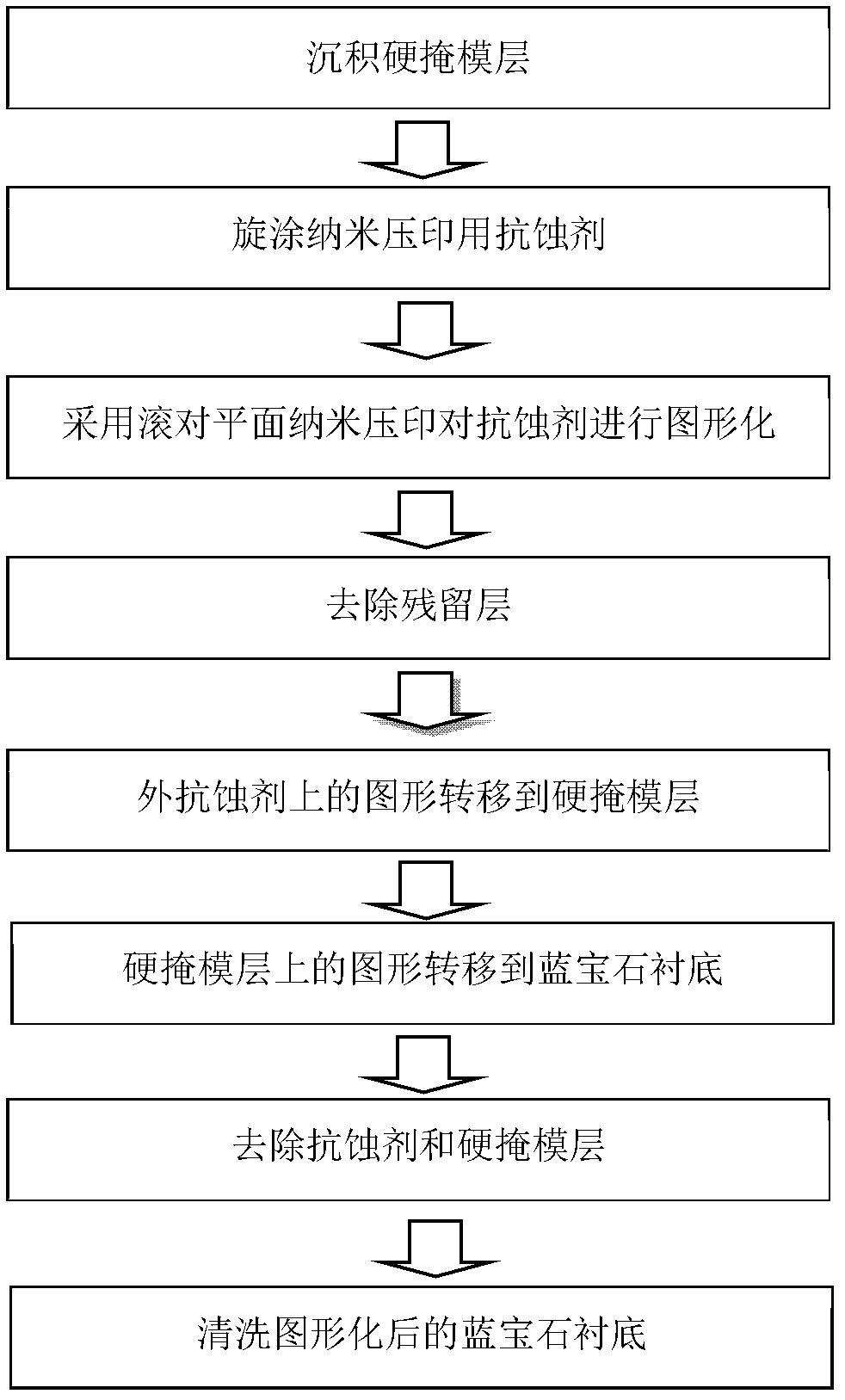
[0051] The present invention will be further described in detail below in conjunction with the accompanying drawings and the embodiments given by the inventor according to the technical solution of the present invention.

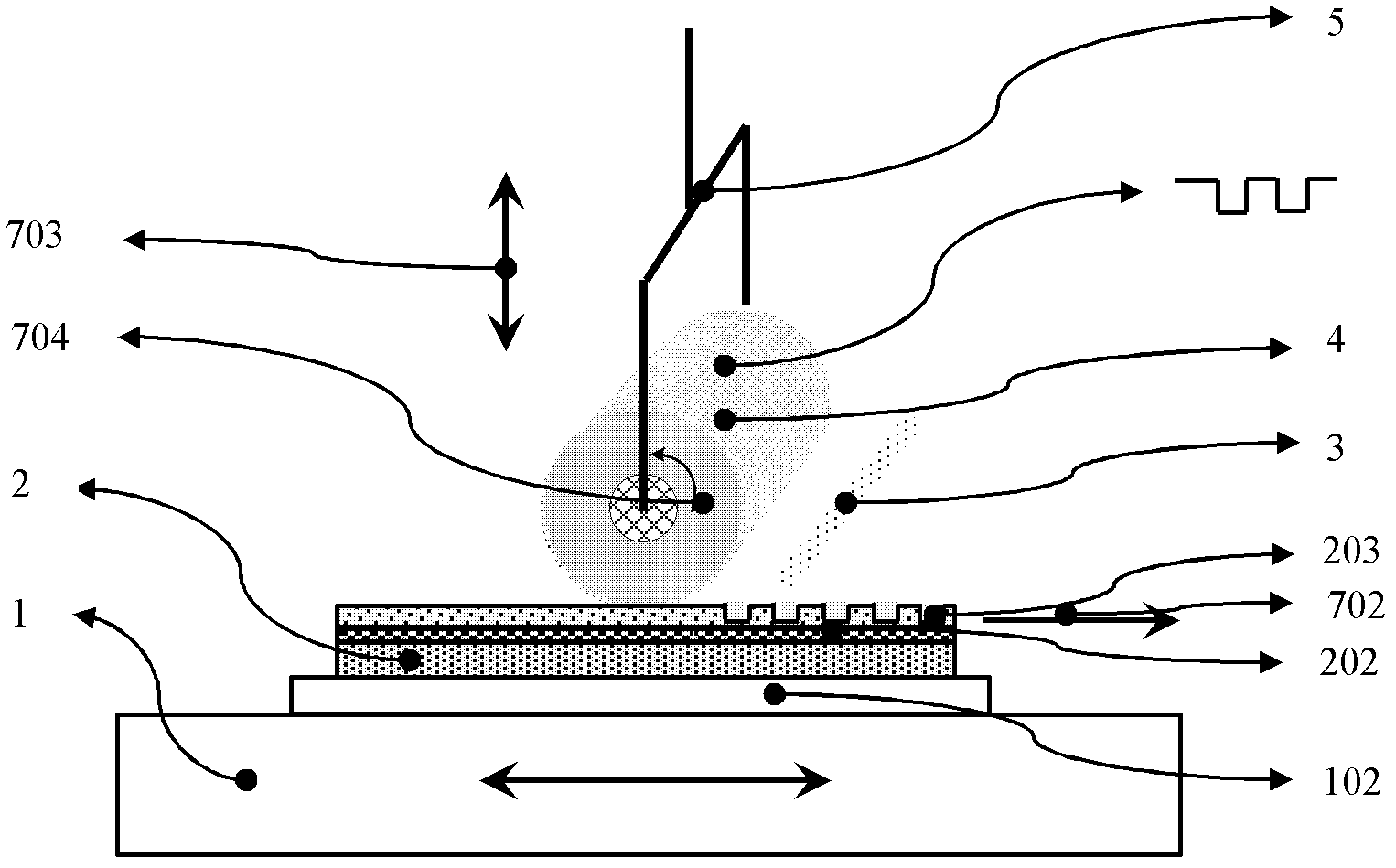
[0052] figure 1 , figure 2 In the present invention, a 4-inch (about 100 mm) nano-patterned sapphire substrate 2 is taken as an example to describe in detail the manufacturing device and method for realizing wafer-level nano-patterned sapphire substrates using the roll-to-plane nanoimprint process.

[0053] A large-scale wafer-level nano-patterned sapphire substrate imprinting device, which includes: a workbench 1 that carries a sapphire substrate 2 and moves in the x-y direction, and is provided with a resist 203 on the workbench 1 The sapphire substrate 2, above the sapphire substrate 2, is provided with a roller-type imprinting mold 4 for longitudinal imprinting along the z-axis 703, and the roller-type imprinting mold 4 is connected to the imprinting m...


PUM

PropertyMeasurementUnit
diameteraaaaaaaaaa
heightaaaaaaaaaa
diameteraaaaaaaaaa

Abstract

The invention discloses a large-size wafer level nano-patterned sapphire substrate imprinting device and method. The method is characterized by (1) depositing a hard mask layer and spin-coating a resist for nanoimprint on the sapphire substrate; (2) adopting a roll-to-flat nanoimprint process and device to pattern the resist; (3) transferring the patterns on the resist to the hard mask layer and the sapphire substrate; and (4) removing the resist and the hard mask layer and washing the patterned sapphire substrate. The device and the method can be used for patterned manufacturing of the substrates made of silicon carbide, silicon, gallium arsenide, gallium nitride and other materials and manufacturing of such micro-nano structures as solar cells, fuel cell bipolar plates, micro-optical lenses, micro-fluidic devices and the like. The device has the characteristics of simple structure, low cost, high productivity, large imprint area and suitability for scale manufacturing.

Description

technical field [0001] The present invention relates to a patterned sapphire substrate method, in particular to a device and method for realizing a large-size wafer-level nano-patterned sapphire substrate imprinting device and method using a roll-to-plane nanoimprinting method, which belongs to micro-nano manufacturing and optoelectronic device manufacturing technology. Background technique [0002] Sapphire substrate is currently the most important substrate for manufacturing blue, green and white group-III nitride LEDs. Compared with other substrates (such as silicon carbide, silicon, GaN, etc.), it has mature manufacturing technology, low single-chip cost, With the advantages of good chemical and temperature stability, good mechanical properties, and no absorption of visible light, it is currently the most widely used substrate in the LED industry. However, as the mainstream substrate in the LED industry, the sapphire substrate has a major defect: there is a large lattic...

Claims


Application Information

Patent Timeline
Patent Type & Authority Applications(China)
IPC IPC(8): G03F7/00G03F7/20H01L33/00
Inventor 兰红波丁玉成
Owner 兰红波
Why Eureka
Try Eureka