P-type conductive zinc oxide film material and preparation method thereof

A technology of conductive zinc oxide and thin film materials, applied in the field of nanomaterials, can solve the problems of low carrier mobility, unstable ZnO acceptor impurities, and low carrier concentration, and achieve high carrier concentration and stable empty space. The effect of hole conduction and increasing doping concentration

Inactive Publication Date: 2012-03-21
SUN YAT SEN UNIV
View PDF6 Cites 16 Cited by
  • Summary
  • Abstract
  • Description
  • Claims
  • Application Information

AI Technical Summary

Problems solved by technology

[0008] To sum up, the disadvantages of realizing p-type ZnO conduction at present are: low carrier concentration and low c

Method used


Image

  • P-type conductive zinc oxide film material and preparation method thereof
  • P-type conductive zinc oxide film material and preparation method thereof
  • P-type conductive zinc oxide film material and preparation method thereof

Examples


Example Embodiment

[0039] Example 1

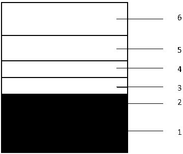
[0040] Such as figure 1 As shown, a p-type conductive zinc oxide thin film material includes a substrate 1 and an epitaxial layer grown on the substrate. A metal magnesium layer 2 and magnesium oxide are sequentially arranged between the substrate and the epitaxial layer from bottom to top. Layer 3, the first zinc oxide layer 4 and the second zinc oxide layer 5 with gradually increasing growth temperature; the epitaxial layer is a p-type BeZnO formed by doping an acceptor element N and doping Be atoms in a zinc oxide alloy: N-layer 6. The p-type ZnO conductive film is in a single crystal state through XRD test, and its rocking curve scan half-height FWHM is 0.09°. Among them, the material of the substrate 1 is sapphire. The thickness of the magnesium metal layer 2 is 0.5 nm. The thickness of the magnesium oxide layer is 2 nm. The thickness of the first zinc oxide layer 4 is 1.5 nm. The thickness of the second zinc oxide layer 5 is 30 nm. The thickness of...

Example Embodiment

[0055] Example 2

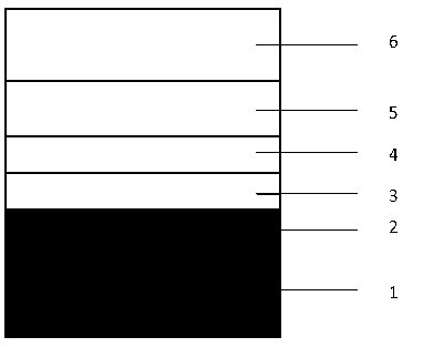
[0056] Such as figure 2 As shown, a p-type conductive zinc oxide thin film material includes a substrate 1 and an epitaxial layer grown on the substrate. A metal magnesium layer 2 and magnesium oxide are sequentially arranged between the substrate and the epitaxial layer from bottom to top. Layer 3, the first zinc oxide layer 4 and the second zinc oxide layer 5 with gradually increasing growth temperature; the epitaxial layer is a p-type BeZnO formed by doping an acceptor element N and doping Be atoms in a zinc oxide alloy: N-layer 6. The p-type ZnO conductive film is in a single crystal state through XRD testing, and its rocking curve scan half-height FWHM is 0.08°. Among them, the material of the substrate 1 is sapphire. The thickness of the magnesium metal layer 2 is 0.7 nm. The thickness of the magnesium oxide layer is 2 nm. The thickness of the first zinc oxide layer 4 is 2 nm. The thickness of the second zinc oxide layer 5 is 33 nm. The thickness o...

Example Embodiment

[0071] Example 3

[0072] Such as image 3 As shown, a p-type conductive zinc oxide thin film material includes a substrate 1 and an epitaxial layer grown on the substrate. A metal magnesium layer 2 and magnesium oxide are sequentially arranged between the substrate and the epitaxial layer from bottom to top. Layer 3, the first zinc oxide layer 4 and the second zinc oxide layer 5 with gradually increasing growth temperature; the epitaxial layer is a p-type BeZnO formed by doping an acceptor element N and doping Be atoms in a zinc oxide alloy: N-layer 6. The p-type ZnO conductive film is in a single crystal state through XRD test, and its rocking curve scan half-height FWHM is 0.085°. Among them, the material of the substrate 1 is sapphire. The thickness of the magnesium metal layer 2 is 1 nm. The thickness of the magnesium oxide layer is 3 nm. The thickness of the first zinc oxide layer 4 is 2 nm. The thickness of the second zinc oxide layer 5 is 27 nm. The thickness of th...


PUM

PropertyMeasurementUnit
Thicknessaaaaaaaaaa
Thicknessaaaaaaaaaa
Thicknessaaaaaaaaaa

Abstract

The invention discloses a p-type conductive zinc oxide film material, which comprises a substrate and an epitaxial layer growing on the substrate, wherein a metal magnesium layer, a magnesium oxide layer, a first zinc oxide layer and a second zinc oxide layer are arranged in sequence between the substrate and the epitaxial layer; the growth temperatures of the first and the second zinc oxide layers are gradually increased; and the epitaxial layer is a p-type AZnO:B layer formed by a zinc oxide alloy doped with acceptor element B and A atoms. The p-type conductive zinc oxide film material and the preparation method thereof have the advantages that the stable hole conduction with high-carrier concentration is achieved by introducing A atoms into ZnO to form AZnO alloy and then doping acceptor element B in the alloy. In the invention, the Zn atoms are replaced by the introduced A atoms, and after the A atoms bond with the acceptor atoms B, since the energy of A-B bonds is very strong as compared with that of the Zn-B bonds, the A atoms can effectively trap the acceptor B atoms to prevent instability due to the Zn-B bond rupture during the process of directly doping the acceptor B atoms in ZnO. Besides, the introduction of A atoms increases the doping concentration of acceptor B atoms, so as to ensure high-concentration and stable hole conduction.

Description

Technical field [0001] The invention relates to the technical field of nanomaterials, in particular to a p-type conductive zinc oxide film material and a preparation method. Background technique [0002] Due to its large band gap and large exciton binding energy, ZnO can realize exciton recombination luminescence at room temperature. This method has the advantages of high quantum efficiency and low threshold, so ZnO is considered to be the material of choice for next-generation optoelectronic devices. Due to crystal defects in intrinsic ZnO and unintentional doping, intrinsic ZnO exhibits n-type conductivity. At present, the main reason that restricts the application of ZnO to semiconductor optoelectronic devices is the inability to achieve stable, high carrier concentration p-type conductivity. [0003] At present, there are four main methods for realizing ZnO p-type conductivity: [0004] First, ZnO is directly doped with group V elements N, P or As, group V elements occupy the ...

Claims


Application Information

Patent Timeline
IPC IPC(8): H01L31/0296H01L31/20H01L21/36
CPCY02P70/50
Inventor 汤子康陈明明苏龙兴张权林祝渊吴天准桂许春项荣
Owner SUN YAT SEN UNIV
Why Eureka
Try Eureka