Production method of low-noise germanium-silicon heterojunction bipolar transistor

A technology of heterojunction bipolar and manufacturing method, which is applied in semiconductor/solid-state device manufacturing, electrical components, circuits, etc. It can solve the problems of increased 1/f noise of noisy devices, low current amplification of HBT, and increased white noise of devices, etc. , to achieve the effect of improving noise characteristics, reducing defect density and surface state

Active Publication Date: 2012-04-11
SHANGHAI HUAHONG GRACE SEMICON MFG CORP
View PDF5 Cites 4 Cited by
  • Summary
  • Abstract
  • Description
  • Claims
  • Application Information

AI Technical Summary

Problems solved by technology

[0002] A very important application field of silicon germanium heterojunction bipolar transistor (SiGe HBT) is the low noise amplifier, which takes full advantage of the low noise advantage of silicon germanium heterojunction bipolar transistor (SiGe HBT). Bipolar transistors (SiGe HBT) generally use polysilicon emitters, which are easier to form crystal defects and surface states at the emitter / base junction, and the 1 / f noise of noisy devices increases, thereby increasing the white noise of the device
However, the emitter cannot use a silicon single crystal layer, because the N-type impurities in the emitter cannot form a relatively uniform distribution in the silicon single crystal layer, which will reduce the injection efficiency of carriers from the emitter region to the base region, resulting in HBT. low current magnification
Therefore, low noise and high current amplification have become a pair of contradictions in the performance parameters of SiGe HBT devices.

Method used


Image

  • Production method of low-noise germanium-silicon heterojunction bipolar transistor
  • Production method of low-noise germanium-silicon heterojunction bipolar transistor
  • Production method of low-noise germanium-silicon heterojunction bipolar transistor

Examples


Embodiment Construction

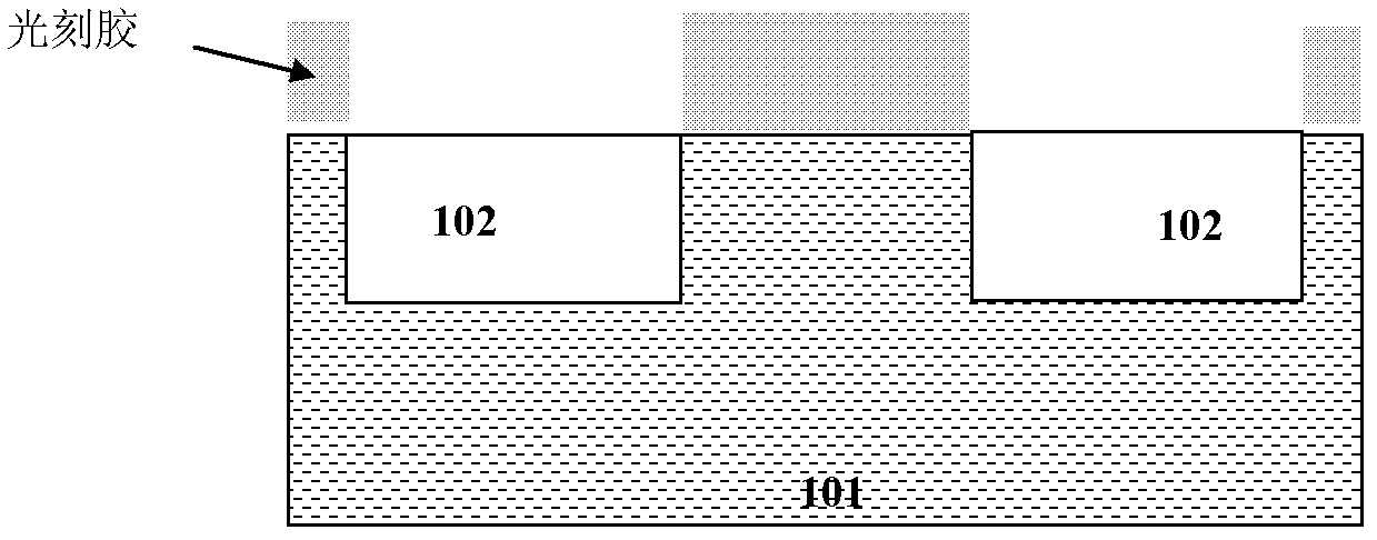
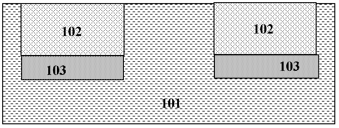
[0029] In the present invention, the emitter of the silicon germanium HBT still adopts the conventional polysilicon thin film, but after carrying out ion implantation doping to the polysilicon emitter and performing rapid thermal annealing impurity redistribution, the polysilicon emitter is carried out pre-amorphization ion implantation ( PAI), and rapid annealing (RTA), to achieve recrystallization of the amorphized emitter, to generate a single crystal layer, so that the emitter / base junction is composed of single crystal silicon / single crystal germanium silicon, improving the noise characteristics of the device. Because the diffusion and redistribution of impurities in the emitter has been completed before PAI, the recrystallization of PAI and RTA will not affect the distribution of impurities in the emitter, and will not change the current amplification factor of HBT.

[0030] The manufacturing process of the low-noise SiGe HBT may include the following steps:

[0031] 1. ...


PUM


Abstract

The invention discloses a production method of a low-noise germanium-silicon heterojunction bipolar transistor, comprising the following steps of: step 1, applying a polysilicon layer for an emitting electrode of the germanium-silicon heterojunction bipolar transistor, doping the emitting electrode, then, executing quick thermal annealing, and diffusing and redistributing the impurities; step 2, executing pre-amorphization ion implantation with medium and high dosage of large atom impurities on the polysilicon emitting electrode, annealing quickly, realizing re-crystallization of the amorphous emitting electrode, and generating a single crystal layer, thereby forming an emitting area / base area junction by the monocrystal silicon / monocrystal germanium and silicon; step 3, executing quick thermal annealing after the process of pre-amorphization ion implantation, and crystallizing the amorphous emitting electrode. With the method provided by the invention, the noise caused by a polysilicon emitting electrode is reduced, and noise characteristics of devices are improved.

Description

technical field [0001] The invention relates to a method for manufacturing a semiconductor device, in particular to a method for manufacturing a germanium-silicon heterojunction bipolar transistor. Background technique [0002] A very important application field of silicon germanium heterojunction bipolar transistor (SiGe HBT) is the low noise amplifier, which takes full advantage of the low noise advantage of silicon germanium heterojunction bipolar transistor (SiGe HBT). Bipolar transistors (SiGe HBT) generally use polysilicon emitters, which are relatively easy to form crystal defects and surface states at the emitter / base junction, and the 1 / f noise of noisy devices increases, thereby increasing the white noise of the device. However, the emitter cannot use a silicon single crystal layer, because the N-type impurities in the emitter cannot form a relatively uniform distribution in the silicon single crystal layer, which will reduce the injection efficiency of carriers fr...

Claims


Application Information

Patent Timeline
IPC IPC(8): H01L21/331
Inventor 钱文生
Owner SHANGHAI HUAHONG GRACE SEMICON MFG CORP
Why Eureka
Try Eureka