Advanced four-side flat pin-free package and manufacturing method thereof

A leadless packaging, four-sided flat technology, applied in semiconductor/solid-state device manufacturing, electrical components, electric solid-state devices, etc., can solve problems such as limiting the number of I/O, shortening the life of cutting blades, pin failure, etc., to prevent The failure of pin welding, the improvement of surface mount quality, and the effect of preventing chip drift

Inactive Publication Date: 2012-04-18
BEIJING UNIV OF TECH
View PDF4 Cites 6 Cited by
  • Summary
  • Abstract
  • Description
  • Claims
  • Application Information

AI Technical Summary

Problems solved by technology

[0004] With the improvement of IC integration and the continuous enhancement of functions, the number of I / Os of ICs increases, and the number of I / O pins of corresponding electronic packages also increases accordingly. The pins of the ring are arranged around the chip carrier, which limits the increase in the number of I / Os and cannot meet the needs of high-density ICs with more I / Os.
The traditional lead frame has no step structure design, which cannot effectively lock the plastic material, resulting in low bonding strength between the lead frame and the plastic packaging material, which is easy to cause delamination of the lead frame and the plastic packaging material or even the falling off of the pin or chip carrier, and cannot effectively Prevent moisture from diffusing into the electronic package along the interface between the lead frame and the plastic packaging material, which seriously affects the reliability of the package
The chip carrier and outer pins of traditional QFN products do not have a certain raised part, and the solder coverage area is limited during surface mounting, and the thickness of the solder is thinner, resulting in a shorter fatigue life of the board-level package and thinner soldering Due to the large thermal strain caused by the thermal mismatch of the layer, it is easy to cause the fracture and delamination failure of the soldering layer, which affects the reliability of the soldering layer
Because the size of the traditional QFN product carrier is much larger than the size of the pins arranged around the periphery, when it is soldered on a circuit board such as a PCB, the large area of ​​solder under the chip carrier is likely to cause the drift of the package, resulting in the soldering of the pins arranged around the periphery. failure of
Traditional QFN products need to paste tape on the back of the lead frame in advance to prevent overflow during the plastic packaging process. After plastic packaging, cleaning processes such as removing the tape and molding compound flash need to be performed, which increases the packaging cost.
Use a dicing knife to cut and separate traditional quad flat no-lead packages. The dicing knife will also cut the lead frame metal while cutting the plastic packaging material, which will not only reduce the cutting efficiency and shorten the life of the dicing blade, but also produce metal burrs. , affecting the reliability of the package

Method used


Image

  • Advanced four-side flat pin-free package and manufacturing method thereof
  • Advanced four-side flat pin-free package and manufacturing method thereof
  • Advanced four-side flat pin-free package and manufacturing method thereof

Examples


Embodiment Construction

[0071] The present invention is described in detail below in conjunction with accompanying drawing:

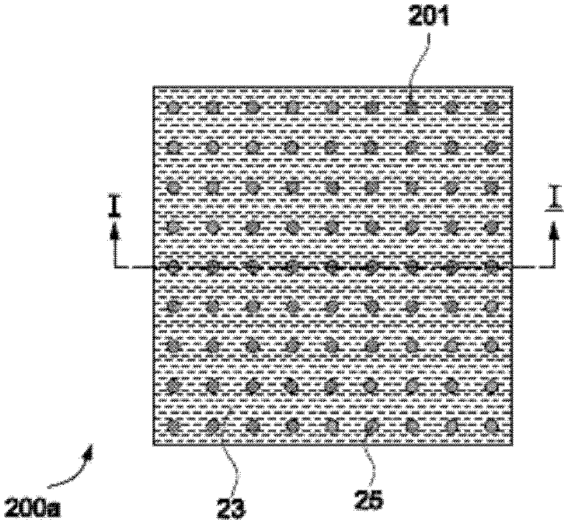
[0072] Figure 2A A schematic diagram of the rear side of an advanced QFN package structure in which the cross-section of the pins is circular and the pins are arranged in parallel in an area array pin arrangement according to an embodiment of the present invention. Figure 2B A schematic diagram of the rear side of an advanced QFN package structure in which the cross-section of the pins is rectangular and the pins are arranged in parallel in an area array pin arrangement according to an embodiment of the present invention.

[0073] Refer to the above Figure 2A -B It can be seen that, in this embodiment, the advanced QFN package structures 200a and 200b arranged in an area array have pins 201 arranged in an area array, and the arrangement of the pins 201 is parallel. A metal material layer 25 is disposed on the lower surface of the pins 201 , and an insulating filling mater...


PUM


Abstract

The invention discloses an advanced four-side flat pin-free package and a manufacturing method thereof. The advanced four-side flat pin-free package comprises a chip carrier, pins, a metal material layer, an IC (Integrated Circuit) chip, insulated filling materials, a bonding material, a metal wire and a plastic sealing material, wherein the chip carrier is provided with a groove structure and the pins for grounding; and the pins are arranged in a package structure in a plane array form. The metal material layer is configured at the upper surfaces and the lower surfaces of the chip carrier and the pins; the IC chip is configured on the metal material layer at the upper surface of the chip carrier, or configured on the metal material layers at the upper surfaces of the pins; and the insulated filling materials are configured below stepped structures of the plurality of chips and a groove of the chip carrier. A package part is formed by coating and sealing the plastic sealing material; and the chip carrier and the external pins which are exposed out of the bottom surface of a package part structure are provided with protruded parts. According to the advanced four-side flat pin-free package and the manufacturing method thereof disclosed by the invention, the bottleneck of less I / O (Input / Output) is broken through and the reliability of the package is improved.

Description

technical field [0001] The invention relates to the technical field of manufacturing semiconductor components, in particular to an advanced quadrilateral flat no-lead package, and the invention also includes a manufacturing method of the package. Background technique [0002] With the development of electronic products such as mobile phones and notebook computers towards miniaturization, portability, ultra-thinness, multimedia and low-cost requirements for popularization, high-density, high-performance, high-reliability and low-cost packaging forms and Its assembly technology has been developed rapidly. Compared with the expensive BGA and other packaging forms, the new packaging technology developed rapidly in recent years, that is, the quad flat non-lead QFN (Quad Flat Non-lead Package) package, due to its good thermal performance and electrical performance, small size, Many advantages such as low cost and high productivity have triggered a new revolution in the field of m...

Claims


Application Information

Patent Timeline
Patent Type & Authority Applications(China)
IPC IPC(8): H01L23/495H01L23/31H01L21/56H01L21/60
CPCH01L2224/32245H01L24/97H01L2224/97H01L2224/73265H01L2224/48247H01L2924/3011H01L2924/30107H01L24/73H01L2924/14H01L2924/181H01L2224/85H01L2924/00012H01L2924/00
Inventor 秦飞夏国峰安彤武伟刘程艳朱文辉
Owner BEIJING UNIV OF TECH
Why Eureka
Try Eureka