Processing agent composition for semiconductor surface and method for processing semiconductor surface using same

A composition and semiconductor technology, which can be used in the preparation of detergent mixture compositions, detergent compositions, chemical instruments and methods, etc., and can solve the problems of complicated procedures and difficulty in peeling off the anti-reflection film layer.

Inactive Publication Date: 2012-05-30
WAKO PURE CHEMICAL INDUSTRIES
View PDF7 Cites 10 Cited by
  • Summary
  • Abstract
  • Description
  • Claims
  • Application Information

AI Technical Summary

Problems solved by technology

[0003] On the other hand, various resist strippers (for example, Patent Document 1, Patent Document 2, etc.) have been known so far. The substrate with anti-reflection film layer is effective, but for the substrate coated with anti-reflection film layer, there is a problem that although the resist layer can be peeled off, it is difficult to peel off the anti-reflection film layer. When stripping the two layers of res

Method used


Image

  • Processing agent composition for semiconductor surface and method for processing semiconductor surface using same
  • Processing agent composition for semiconductor surface and method for processing semiconductor surface using same
  • Processing agent composition for semiconductor surface and method for processing semiconductor surface using same

Examples


Embodiment 1

[0078] Embodiment 1 Preparation of semiconductor surface treatment agent composition (1) of the present invention

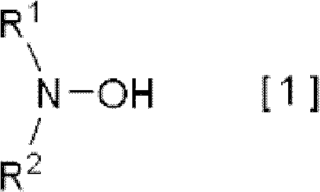
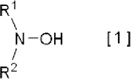
[0079] For a solution of 4.74 g of water and 1.29 g of sodium alkyl sulfosuccinate (Neocol P; manufactured by Daiichi Kogyo Pharmaceutical Co., Ltd.), under a yellow lamp (straight tube yellow fluorescent lamp, FLR40SY-IC / M; Mitsubishi Electric OSRAM Co., Ltd. 0.06 g of ammonium fluoride and 0.5 g of 2-benzyl-2-dimethylamino-1-(4-morpholinephenyl)-butanone-1 (Irgacure 369; manufactured by Ciba Seika Co., Ltd.) were added under the irradiation of g, stirred at room temperature. After confirming the dissolution of ammonium fluoride and Irgacure 369, the stirring was continued, 93 g of γ-butyrolactone was added to the solution, and 0.01 g of diethylhydroxylamine was added, followed by 0.4 g of citric acid to prepare a combination of the present invention at pH 2 thing (1).

Embodiment 2~18

[0080] Embodiments 2-18 Preparation of semiconductor surface treatment agent compositions (2)-(18) of the present invention

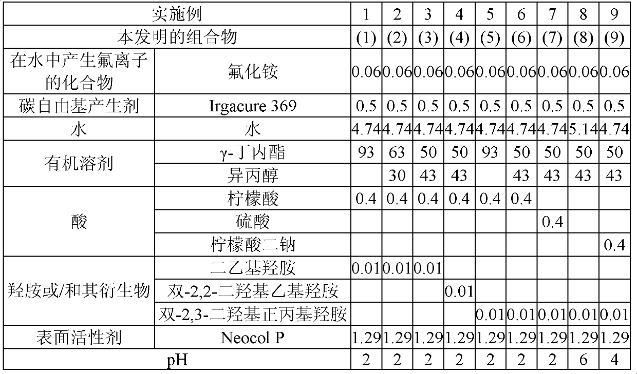
[0081] In Examples 2 to 18, compositions (2) to (18) of the present invention were prepared in the same manner as in Example 1, except that the components shown in Table 1 and Table 2 were used and the amounts shown in Table 1 and Table 2 were added. ). Their compositions are listed in Table 1 and Table 2 together with the composition of Example 1. In addition, the numerical value shown in Table 1 and Table 2 is the weight% density|concentration of each component when the total weight of a composition is assumed as 100%.

[0082] [Table 1]

[0083]

[0084] Irgacure 369: 2-Benzyl-2-dimethylamino-1-(4-morpholinephenyl)-butanone-1

[0085] Neocol P: sodium alkyl sulfosuccinate

[0086] [Table 2]

[0087]

[0088] Irgacure 369: 2-Benzyl-2-dimethylamino-1-(4-morpholinephenyl)-butanone-1

[0089] VA-057: 2,2'-Azobis[N-(2-carboxyethyl)-2-methylpro...

Embodiment 19

[0097] Example 19 Evaluation of the semiconductor surface treatment agent composition (1) of the present invention

[0098] For 50 mL of the composition (1) of the present invention prepared in Example 1, an ultraviolet irradiation device (UV irradiation device, MUV-35U MUV-PF001 with color filter; manufactured by Moritex Co., Ltd.) was used at room temperature with a center wavelength of 320 nm. The above-mentioned substrate sample for evaluation was immersed for 3 minutes under gentle stirring while irradiating with light. Thereafter, the substrate surface was rinsed with pure water for 30 seconds and dried with compressed air. As a result of observing the dried substrate sample visually and with a field emission scanning electron microscope (S-4800; manufactured by Hitachi High-Technologies Co., Ltd.), it was confirmed that the resist layer and the cured resist layer were well peeled off. There is no residue, and more than 90% of the anti-reflection film layer has been pee...


PUM


Abstract

Disclosed are: a processing agent composition for semiconductor surfaces, which is capable of easily removing an antireflective film layer, a resist layer and a resist cured layer in a short time during the production procedure of a semiconductor element or the like; and a method for processing a semiconductor surface, which is characterized by using the processing agent composition. Specifically disclosed is a processing agent composition for semiconductor surfaces, which is characterized by containing (I) a compound which generates fluorine ions in water, (II) a carbon radical generator, (III) water, (IV) an organic solvent and (V) at least one compound selected from the group consisting of hydroxylamines and hydroxylamine derivatives represented by general formula (1). Also specifically discloses is a method for processing a semiconductor surface, which is characterized by using the processing agent composition. (In the formula, R1 represents a linear, branched or cyclic alkyl group with 1-6 carbon atoms or a linear or branched substituted alkyl group with 1-4 carbon atoms having 1-3 hydroxyl groups; and R2 represents a hydrogen atom, a linear, branched or cyclic alkyl group with 1-6 carbon atoms or a linear or branched substituted alkyl group with 1-4 carbon atoms having 1-3 hydroxyl groups).

Description

technical field [0001] The present invention relates to a semiconductor surface treating agent composition and a semiconductor surface treating method using the composition. More specifically, the present invention relates to the following semiconductor surface treatment agent composition and the treatment method of semiconductor surface: said semiconductor surface treatment agent composition can peel off the anti-reflection film layer in the manufacturing process of semiconductor element etc., further ground, it can not only peel off the anti-reflection film layer, but also can peel off the resist layer as the upper layer of the anti-reflection film layer and the resist cured layer produced in the etching process; the processing method of the semiconductor surface is characterized in that it uses the above-mentioned combination. Background technique [0002] In the prior art, semiconductor elements such as ICs and LSIs are manufactured as follows: a conductive metal film, ...

Claims


Application Information

Patent Timeline
IPC IPC(8): H01L21/304G03F7/42H01L21/027H01L21/306
CPCG03F7/425H01L21/31133G03F7/426G03F7/423C11D11/0047
Inventor 水田浩德木村卓博
Owner WAKO PURE CHEMICAL INDUSTRIES
Why Eureka
Try Eureka