GaN-based light-emitting diode (LED) epitaxial wafer capable of improving luminous efficiency, and preparation method and application thereof

A technology of LED epitaxial wafers and luminous efficiency, applied in the field of optoelectronics, can solve the problems of lower product yield, complicated process, quantum well damage, etc., and achieve the effects of cost reduction, simple process, and improved luminous efficiency

Active Publication Date: 2012-06-06
HUAWEI TEHCHNOLOGIES CO LTD
View PDF7 Cites 8 Cited by
  • Summary
  • Abstract
  • Description
  • Claims
  • Application Information

AI Technical Summary

Problems solved by technology

The process of this method is relatively complicated, and it is easy to reduce the yield of the product; and dry etching or high temperature corrosion will cause damage to the quantum well

Method used


Image

  • GaN-based light-emitting diode (LED) epitaxial wafer capable of improving luminous efficiency, and preparation method and application thereof
  • GaN-based light-emitting diode (LED) epitaxial wafer capable of improving luminous efficiency, and preparation method and application thereof
  • GaN-based light-emitting diode (LED) epitaxial wafer capable of improving luminous efficiency, and preparation method and application thereof

Examples


Embodiment 1

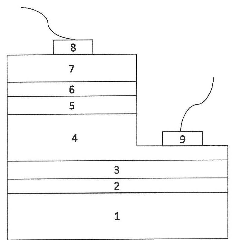
[0042] Embodiment 1: A GaN-based LED epitaxial wafer on a sapphire substrate is grown according to the following steps:

[0043] (1) Put the sapphire substrate 1 into the reaction chamber of the MOCVD equipment, heat it to 1150° C. under the hydrogen atmosphere, and process it for 15 minutes.

[0044] (2) growing a gallium nitride buffer layer 2 on the substrate at a growth temperature of 550° C. and a thickness of 30 nm;

[0045] (3) Non-doped GaN 3 and N-type GaN 4 are grown on the buffer layer 2 at a growth temperature of 1100° C., and the growth thicknesses are respectively 2 μm for non-doped GaN and 3 μm for N-type GaN. The silicon doping concentration of N-type GaN 4 is 1×10 19 / cm -3 .

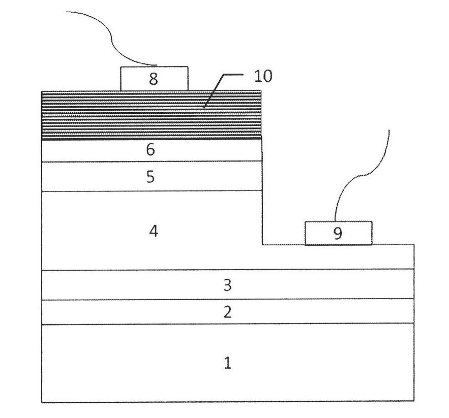
[0046] (4) The multi-quantum well structure 5 is grown on the N-type gallium nitride 4, wherein the well layer is made of indium gallium nitride material, the barrier layer is made of gallium nitride material, the growth temperature is 750° C., and the multi-quantum well growth perio...

Embodiment 2

[0052] Follow the steps below to grow LED epiwafers:

[0053] (1) Put the silicon carbide substrate 1 into the reaction chamber of the MOCVD equipment, heat it to 1120° C. under a hydrogen atmosphere, and process it for 8 minutes.

[0054] (2) An aluminum nitride buffer layer 2 is grown on the aforementioned silicon carbide substrate 1 at a growth temperature of 1000° C. and a thickness of 200 nm.

[0055] (3) growing non-doped gallium nitride 3 and N-type gallium nitride 4 on the buffer layer 2, the growth temperature is 1050°C, and the growth thicknesses are respectively 2 μm for non-doped gallium nitride and 3 μm for N-type gallium nitride; N The silicon doping concentration of type GaN is 2×10 18 / cm -3 .

[0056] (4) The multi-quantum well structure 5 is grown on the N-type gallium nitride 4, the well layer is made of indium gallium nitride material, the barrier layer is made of gallium nitride material, the growth temperature is 750° C., and the repeated growth period...

Embodiment 3

[0060] Embodiment 3: grow LED epitaxial wafer according to the following steps:

[0061] (1) Put the sapphire substrate 1 into the reaction chamber of the MOCVD equipment, heat it to 1140° C. under a hydrogen atmosphere, and process it for 11 minutes.

[0062] (2) An AlGaN buffer layer 2 is grown on the above-mentioned sapphire substrate 1 at a growth temperature of 1000° C. and a thickness of 200 nm.

[0063] (3) Non-doped GaN 3 and N-type GaN 4 are grown on the buffer layer 2 at a growth temperature of 1100° C. and a growth thickness of 2 μm and 3 μm respectively. The silicon doping concentration of N-type GaN is 1×10 19 / cm -3 .

[0064] (4) The multi-quantum well structure 5 is grown on the N-type gallium nitride 4, the well layer is made of indium gallium nitride material, the barrier layer is made of gallium nitride material, the growth temperature is 750° C., and the repeated growth period of the multi-quantum well is 20.

[0065] (5) On the multi-quantum well struc...


PUM


Abstract

The invention relates to a GaN-based light-emitting diode (LED) epitaxial wafer capable of improving the luminous efficiency, and a preparation method and the application thereof. A multicycle repetition structure of Mg-doped InGaN and Mg-doped GaN is used to replace a traditional P-type Mg-doped GaN layer, so on the one hand, higher carrier concentration is produced by utilizing polarization effects of InGaN and GaN, and a nitrogen annealing process does not need to be conducted again, and on the other hand, surface coarsening is realized by utilizing surface cavities produced by the multicycle repetition structure of the InGaN and the GaN, and the luminous efficiency of a GaN LED is improved.

Description

technical field [0001] The invention relates to a method for improving the luminous efficiency of a gallium nitride-based blue-green light-emitting diode, which belongs to the field of optoelectronic technology. Background technique [0002] In recent years, semiconductor light-emitting diodes have received widespread attention, because they have the advantages of small size, high efficiency, and long life. The rapid development of wide bandgap III-V semiconductor materials has enabled the commercialization of high-brightness light-emitting diodes from green light to near-ultraviolet products. At present, light-emitting diodes ranging from ordinary green to ultraviolet are widely used in traffic lights, full-color displays, backlight panels of LCD screens, automotive instruments and interior lights, etc. In recent years, ultraviolet light-emitting diodes have entered the market and are mainly used for the detection of biological particles (such as the detection of bacterial...

Claims


Application Information

Patent Timeline
Patent Type & Authority Applications(China)
IPC IPC(8): H01L33/04H01L33/12H01L33/26H01L33/00
Inventor 曲爽徐现刚李毓锋王成新李树强
Owner HUAWEI TEHCHNOLOGIES CO LTD
Why Eureka
Try Eureka