Optical exposing method, and method for applying optical exposure in preparation of silicon material vertical hollow structure

An optical exposure and hole technology, used in microlithography exposure equipment, photosensitive material processing, manufacturing of microstructure devices, etc., can solve the problems of expensive, difficult to use, and high cost, and achieve low production cost, simple operation, and repeatability. good effect

Active Publication Date: 2012-06-13
INST OF PHYSICS - CHINESE ACAD OF SCI
View PDF5 Cites 5 Cited by
  • Summary
  • Abstract
  • Description
  • Claims
  • Application Information

AI Technical Summary

Problems solved by technology

The production of such graphics is generally through electron beam exposure or ultraviolet exposure technology, of which electron beam exposure is very expensive and limited in practical application
Using the

Method used


Image

  • Optical exposing method, and method for applying optical exposure in preparation of silicon material vertical hollow structure
  • Optical exposing method, and method for applying optical exposure in preparation of silicon material vertical hollow structure
  • Optical exposing method, and method for applying optical exposure in preparation of silicon material vertical hollow structure

Examples


example 1

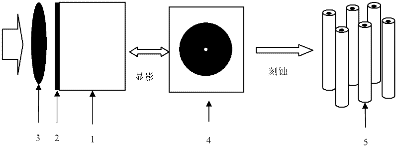
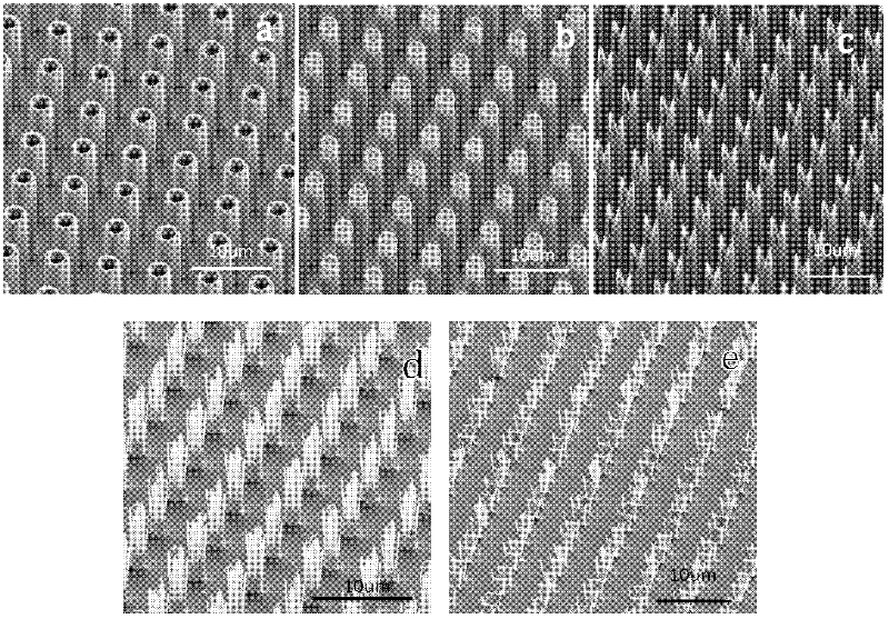
[0057] The silicon tubular array structure prepared in this example is shown in the attached image 3 (a) The silicon tube has a wall thickness of 200 nanometers, an inner diameter of 300 nanometers, and a height of 20 microns. The specific preparation method is as follows:

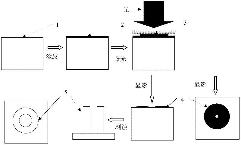
[0058] 1) Surface treatment of silicon wafer: Take a silicon substrate 1 and use a conventional semiconductor cleaning process, that is, ultrasonically clean it in acetone, alcohol and deionized water in sequence, and dry it with nitrogen;

[0059] 2) Glue coating: S1813 photoresist 2 is spin-coated on the silicon substrate 1, and the spin coating speed is controlled to obtain a 500-nanometer thick photoresist coating;

[0060] 3) Pre-baking: Bake the photoresist-coated silicon wafer obtained in step 2) on a hot plate at 150°C for 0.5 minutes;

[0061] 4) Exposure: select a mask 3 with a solid circular array pattern with a radius of 1 micron. Expose on the MA6 UV exposure machine. During the exposure process, th...

example 2

[0065] The silicon tubular array structure prepared in this example is shown in the attached image 3 (b) The silicon tube has a wall thickness of 100 nanometers, an inner diameter of 350 nanometers, and a height of 20 microns. The specific preparation method is as follows:

[0066] 1) Surface treatment of silicon wafer: Take a silicon substrate 1 and use a conventional semiconductor cleaning process, that is, ultrasonically clean it in acetone, alcohol and deionized water in sequence, and dry it with nitrogen;

[0067] 2) Glue coating: S1813 photoresist 2 is spin-coated on the silicon substrate 1, and the spin coating speed is controlled to obtain an 800 nm thick photoresist coating;

[0068] 3) Pre-baking: Bake the photoresist-coated silicon wafer obtained in step 2) on a hot plate at 115°C for 1 minute;

[0069] 4) Exposure: select a mask 3 with a solid circular array pattern with a radius of 1 micron. Expose on the MA6 UV exposure machine. During the exposure process, the Poisson...

example 3

[0073] For the V-shaped tubular array structure of this example, see the attached image 3 (c) The prepared silicon tube has a wall thickness of 100 nanometers, an inner diameter of 350 nanometers, and a height of 30 microns. The specific preparation method is as follows:

[0074] 1) Surface treatment of silicon wafer: Take a silicon substrate 1 and use a conventional semiconductor cleaning process, that is, ultrasonically clean it in acetone, alcohol and deionized water in sequence, and dry it with nitrogen;

[0075] 2) Glue coating: S1813 photoresist 2 is spin-coated on the silicon substrate 1, and the spin coating speed is controlled to obtain an 800 nm thick photoresist coating;

[0076] 3) Pre-baking: Bake the photoresist-coated silicon wafer obtained in step 2) on a hot plate at 115°C for 1 minute;

[0077] 4) Exposure: Select the mask 3 with a solid circular array pattern with a radius of 1 micron, and expose it on the MA6 UV exposure machine. During the exposure process, the P...


PUM

PropertyMeasurementUnit
Wall thicknessaaaaaaaaaa
Diameteraaaaaaaaaa

Abstract

The invention provides an optical exposing method used for forming a micro-nano hollow cavity structure. The method comprises steps that: (1) a mask with a mask pattern is selected, wherein the mask pattern is a geometrical solid pattern or an array thereof with which Poisson spots can be formed through illumination; (2) the mask is positioned above a positive photoresist requiring exposure; exposure is carried out; Poisson spots behind pattern shades are exposed as well; (3) developing is carried out, such that a pattern of hollow cavities corresponding to the Poisson spots is obtained on the positive photoresist. With the method, a silicon pipe-shaped structure array with controllable length-to-diameter ratios can be prepared. With the exposing method, a limit size of laboratory photomask exposure is greatly increased; a limitation of interference exposure that only periodical lines and point lattice can be obtained is broken through; cost is greatly reduced; and experiment technologies are enriched. The structure has a wide application prospect in fields of photonic crystals, filtering devices, and radial p-n junction structured solar cells.

Description

Technical field [0001] The invention belongs to the technical field of micro-nano processing, and in particular relates to an optical exposure method and a method for preparing a vertical silicon material hollow structure array. Background technique [0002] Optical exposure is the earliest microfabrication technology used in semiconductor integrated circuits. At present, optical exposure technology is mainly projection exposure technology, and it is mainly exposure technology for the mass production of integrated circuits. In order to pursue smaller and smaller circuit sizes and the highest possible yield, the development of the technology itself is becoming more and more complicated. The investment required is increasing, and the cost is getting higher and higher. At present, the cost of the most advanced single exposure equipment is 20-50 million US dollars. Only a few large companies in the world can afford to purchase and The cost of running these exposure equipment. The c...

Claims


Application Information

Patent Timeline
IPC IPC(8): G03F7/20G03F7/00G03F7/30B81C1/00
Inventor 顾长志田士兵李俊杰夏晓翔杨海方
Owner INST OF PHYSICS - CHINESE ACAD OF SCI
Why Eureka
Try Eureka