Enhanced protection type toughened low-radiation coated glass and manufacturing process thereof
A technology of low-radiation coating and manufacturing process, which is applied in the direction of sputtering coating, gaseous chemical plating, metal material coating process, etc., can solve the problem of low comprehensive yield, shorten the production cycle, increase the yield of products, The effect of high hardness
- Summary
- Abstract
- Description
- Claims
- Application Information
AI Technical Summary
Problems solved by technology
Method used
Image
Examples
Embodiment 1
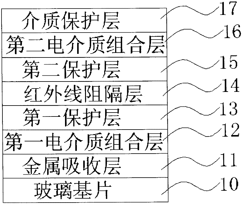
[0057] In this embodiment, the single-silver low-emissivity coated glass is plated by the magnetron sputtering coating method, and then a dielectric protective layer 17 is deposited on the outermost layer of the single-silver low-emissivity coating by radio frequency plasma enhanced chemical vapor deposition. as follows:
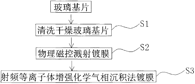
[0058] Executing step S1: cleaning and drying the glass substrate 10;
[0059] Executing step S2: using the magnetron sputtering method to sequentially plate the metal absorption layer 11, the first dielectric composite layer 12, the first protective layer 13, the infrared blocking layer 14, the second protective layer 15, and the second dielectric composite layer 16;
[0060] Step S3 is executed: the dielectric protection layer 17 is deposited by radio frequency plasma enhanced chemical vapor deposition.
[0061] After the plating is completed, wherein, the metal absorption layer 11 is made of stainless steel, preferably SST film, and the thickness of the ...
Embodiment 2
[0082] In this embodiment, the single-silver low-emissivity coated glass is coated by the magnetron sputtering coating method, and then a dielectric protective layer is deposited on the outermost layer of the single-silver low-emissivity coating by radio-frequency plasma-enhanced chemical vapor deposition. The steps are as follows :
[0083] Executing step S1: cleaning and drying the glass substrate 10;
[0084] Executing step S2: using the magnetron sputtering method to plate the metal absorption layer 11, the first dielectric composite layer 12, the first protective layer 13, the infrared blocking layer 14, the second protective layer 15, and the second dielectric composite layer 16;
[0085] Step S3 is executed: the dielectric protection layer 17 is deposited by radio frequency plasma enhanced chemical vapor deposition.
[0086] Wherein, the metal absorption layer 11 is made of stainless steel, specifically an SST film layer, and the thickness of the film layer is: 6nm;
...
PUM
| Property | Measurement | Unit |
|---|---|---|
| thickness | aaaaa | aaaaa |
| thickness | aaaaa | aaaaa |
| thickness | aaaaa | aaaaa |
Abstract
Description
Claims
Application Information


