Method for forming salicide block layer

A metal silicide, barrier layer technology, applied in electrical components, semiconductor/solid-state device manufacturing, circuits, etc., can solve the problems of increased PMOS threshold voltage, uneven threshold voltage, etc., to reduce impact, improve uniformity, high Effect of Extinction Coefficient

Active Publication Date: 2012-07-04
SHANGHAI HUAHONG GRACE SEMICON MFG CORP
View PDF3 Cites 7 Cited by
  • Summary
  • Abstract
  • Description
  • Claims
  • Application Information

AI Technical Summary

Problems solved by technology

like Figure 1i As shown, taking PMOS as an example, electron-hole pairs excited by ultraviolet rays generated by the plasma are injected into the gate oxide layer under an

Method used


Image

  • Method for forming salicide block layer
  • Method for forming salicide block layer
  • Method for forming salicide block layer

Examples


Example Embodiment

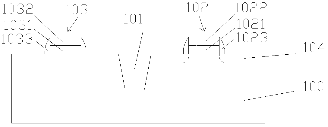
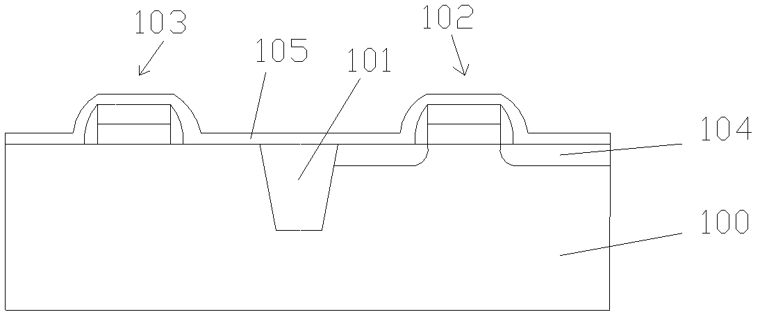
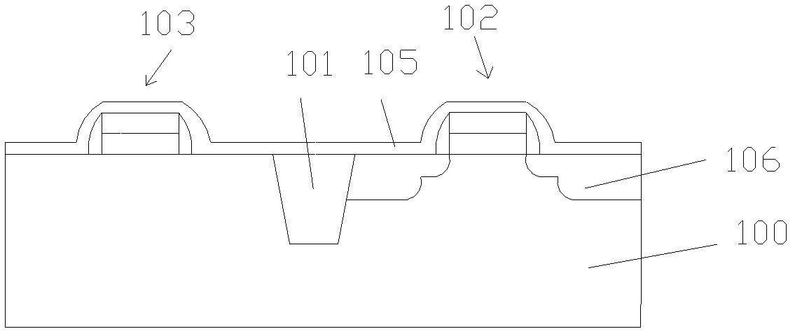
[0026] The present invention will be further detailed below in conjunction with the accompanying drawings:

[0027] In the following description, many specific details are explained in order to fully understand the present invention. However, the present invention can be implemented in many other ways different from those described here, and those skilled in the art can make similar popularizations without violating the connotation of the present invention. Therefore, the present invention is not limited by the specific implementation disclosed below.

[0028] Secondly, the present invention uses schematic diagrams for detailed description. When describing the embodiments of the present invention in detail, the cross-sectional view showing the device structure will not be partially enlarged according to the general scale, and the schematic diagram is only an example, which should not be limited here. The scope of protection of the present invention. In addition, the three-dimensio...


PUM

PropertyMeasurementUnit
Thicknessaaaaaaaaaa

Abstract

The invention relates to a method for forming a salicide block layer. The method comprises the following steps of: providing a substrate, wherein an isolation structure is arranged in the substrate, a first gate structure and a second gate structure are arranged on the surfaces of the substrate on two sides of the isolation structure respectively, and a light doping source and drain injection region is formed in the substrate on the two sides of the first gate structure; depositing a silicon rich oxide (SRO) layer; performing ion implantation on the two sides of the first gate structure so as to form a heavy doping source and drain injection region; depositing a silane layer; coating photoresist, and photoetching to form a first window, wherein an area of the first gate structure is exposed from the first window; removing the silane layer from the first window by dry etching; removing the SRO layer from the first window by wet etching; and removing the photoresist. Due to the adoption of the salicide block layer with the SRO layer and the silane layer, the SRO has a higher extinction coefficient compared with silica, and damage of plasma ultraviolet light to the substrate can be reduced; and therefore, the uniformity of threshold voltage is improved.

Description

Technical field [0001] The invention relates to the field of semiconductors, in particular to a method for forming a metal silicide barrier layer. Background technique [0002] Manufacture of VLSI In the self-aligned refractory metal silicide process, most of the active area is covered by low-resistance refractory metal silicide. However, some areas, such as high-resistance polysilicon and isolated active areas, cannot have refractory metal silicide. These areas need barrier layer protection during the silicide process. It is necessary to form a metal silicide barrier layer (salicide) in this part of the area. block layer, SAB), the metal silicide barrier layer does not react with metals such as titanium or cobalt to prevent the formation of metal silicide in some areas. [0003] In the VLSI manufacturing process, refractory metals such as titanium, cobalt, and nickel are often used to generate silicides. At the same time, silicon dioxide and silane layers are widely used as barr...

Claims


Application Information

Patent Timeline
IPC IPC(8): H01L21/314H01L21/316H01L21/311
Inventor 王卉康军令海阳
Owner SHANGHAI HUAHONG GRACE SEMICON MFG CORP
Why Eureka
Try Eureka