Conductive adhesive for circuit board, single/double-sided multi-layer printed circuit board, and production method

A kind of conductive adhesive and circuit board technology, applied in the field of conductive adhesive, can solve the problems of surface layer copper foil damage, circuit short circuit, affecting resistance value, etc.

Inactive Publication Date: 2012-07-11
吴祖
View PDF2 Cites 26 Cited by
  • Summary
  • Abstract
  • Description
  • Claims
  • Application Information

AI Technical Summary

Problems solved by technology

[0003] For example, the invention patent with the patent number "99106371.6" discloses a conductive adhesive for small hole filling. In order to improve the reliability of thermal shock resistance, the stability of resistance value and the stability of adhesion, the conductive adhesive proposes The lower the viscosity and TI value of the conductive adhesive, the better. Adjust the TI value below 1.0 to enhance the printing effect and make the through holes full. If the conductive adhesive emerges, it is necessary to increase the grinding process to remove the emerging conductive adhesive, otherwise there will be problems such as damage to the copper foil on the surface layer after hot pressing or short circuit caused by overflowing glue.
In addition, in order to increase the adhesion between the substrate and the copper foil, the conductive adhesive sets the carrier-epoxy compound resin ratio to more than 30%. As we all know, conductive substances with high resin content require If the resistance value is reduced accordingly, the resin content is high, and after thermal shock, the expansion rate of the conductive adhesive will be higher, which will further affect the resistance value. In this way, in the actual production operation of the circuit board, the operating parameters of each construction will be The requirements are relatively strict, and a slight deviation will cause defects, which will reduce its quality assurance coefficient and cause a greater potential quality risk
In addition, the metal conductive particles required by the conductive adhesive have an "average particle diameter of 0.5-20um and a specific surface area of ​​0.05-105m 2 / g” also brings a lot of inconvenience in the selection of conductive particles, and the cost rises
In addition, the conductive adhesive is aimed at larger via holes, such as holes above 0.5mm, which are easy to cause air bubbles in the holes, and are easy to burst holes after thermal shock, etc., so that the application range is reduced and the operation convenience is reduced. Happening

Method used


Image

  • Conductive adhesive for circuit board, single/double-sided multi-layer printed circuit board, and production method
  • Conductive adhesive for circuit board, single/double-sided multi-layer printed circuit board, and production method
  • Conductive adhesive for circuit board, single/double-sided multi-layer printed circuit board, and production method

Examples


Embodiment approach 1

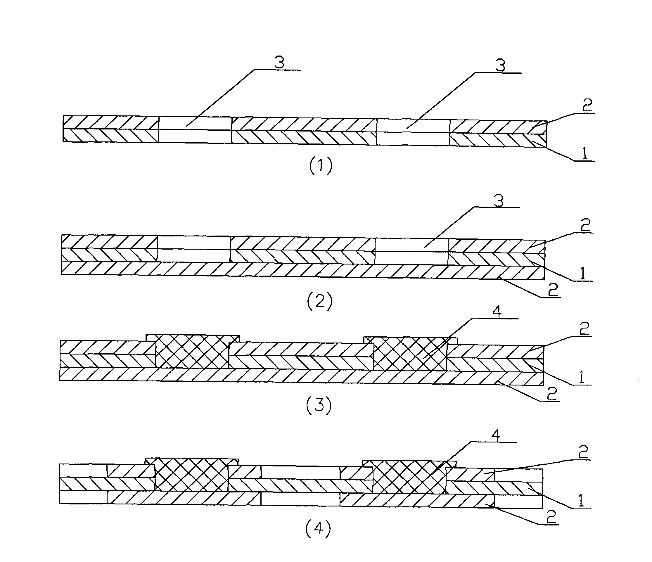
[0071] Implementation plan 1 (production of single-sided panel)

[0072] Substrate: 0.1MM polyimide without hot melt adhesive;

[0073] Printing tool: 77T (ie 200 mesh) screen;

[0074] Operation method:

[0075] 1. After cutting the substrate, remove the dust and oil stains on the surface of the substrate;

[0076] 2. Use 77T screen to print the circuit directly on the surface of the substrate;

[0077] 3. After printing, dry at 130°C-150°C for 30 minutes to obtain the circuit layer;

[0078] 4. Apply the methods known in the industry to make the protective layer and the character layer, and then a complete circuit board can be obtained.

Embodiment approach 2

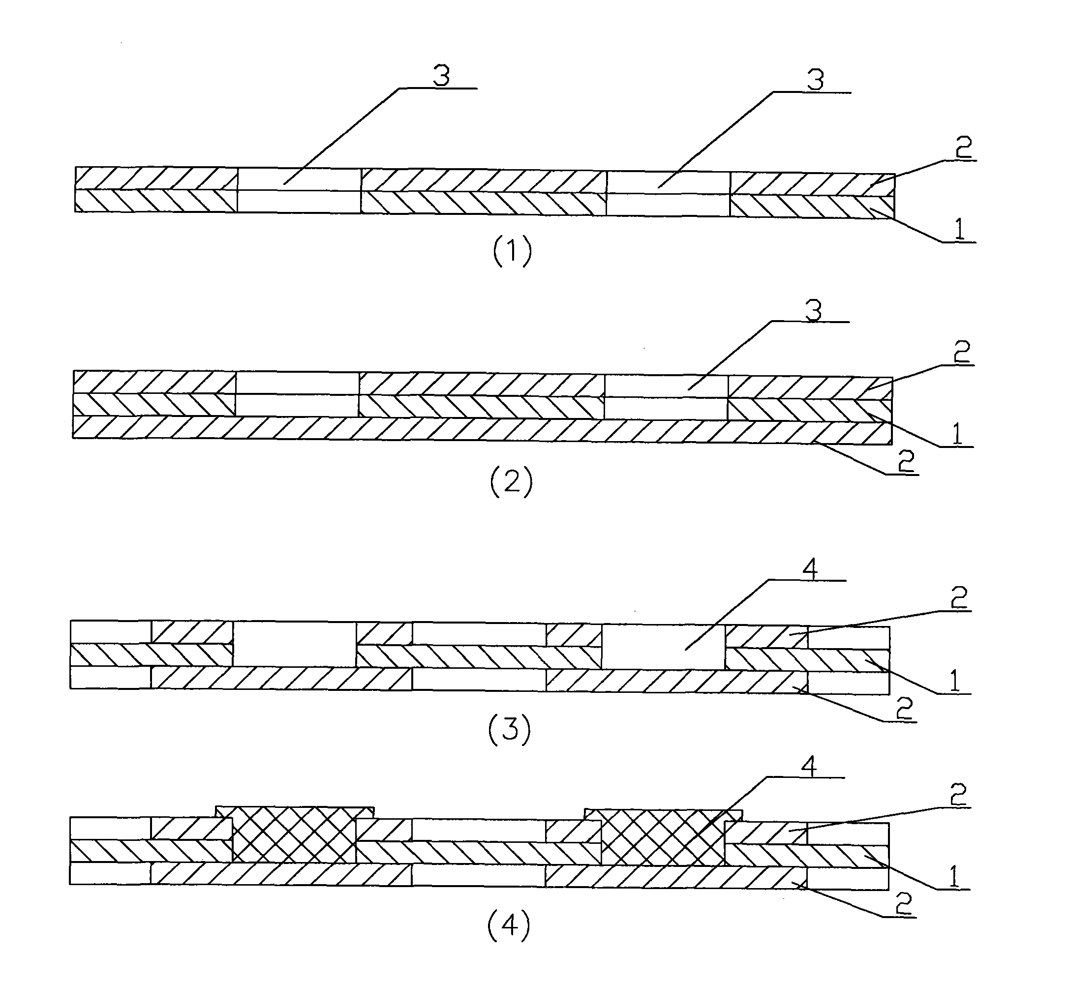
[0079] Implementation plan 2 (one of the production of double-sided panels)

[0080] Substrate: 1. Polyimide substrate coated with semi-cured hot melt adhesive on one side with a thickness of 0.1mm (the thickness of the hot melt adhesive is 30um);

[0081] 2. 18UM copper foil

[0082] Aperture diameter of via hole: 0.5MM

[0083] Printing tool: 77T (ie 200 mesh) screen

[0084] Operation method 1. Firstly, the polyimide base material coated with semi-cured hot-melt resin with a thickness of 30um is first processed by mechanical stamping, mechanical drilling or laser drilling according to the engineering data to process conduction holes and positioning holes, etc.;

[0085] 2. Press the base material with the processed via hole and the copper foil together, the pressing conditions are temperature 180 ℃, pressure 100 kg, time 60 seconds;

[0086] 3. Curing the laminated substrate at 150°C for 60 minutes;

[0087] 4. Use the well-known corrosion method in the industry to make...

Embodiment approach 3

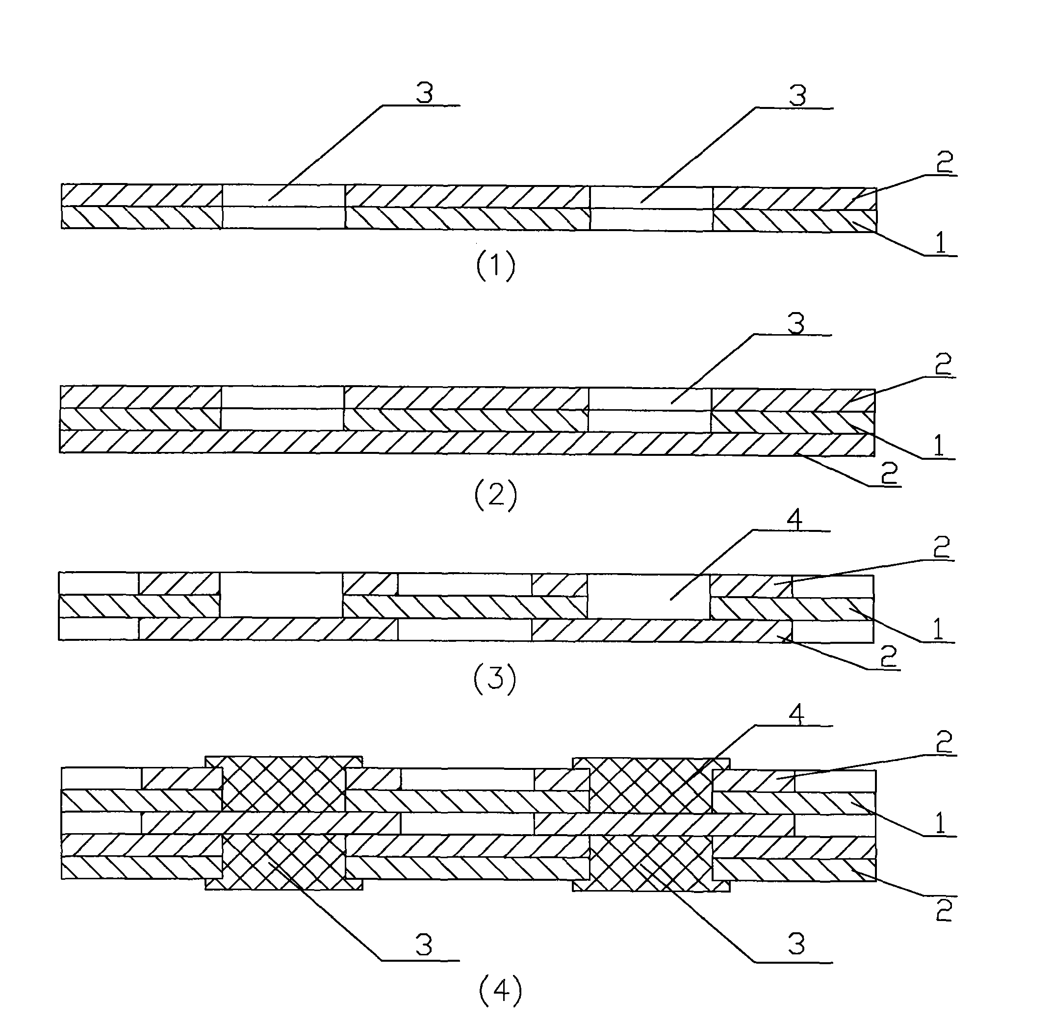
[0091] Implementation plan three (two-sided panel production)

[0092] Substrate: 1. Polyimide substrate coated with semi-cured hot-melt adhesive on both sides with a thickness of 10.1mm (the thickness of the hot-melt adhesive is 30um)

[0093] 2. 18UM copper foil;

[0094] Aperture diameter of via hole: 0.5MM.

[0095] Printing tool: 77T (ie 200 mesh) screen.

[0096] Operation method: 1. Pre-press one side of copper foil on one side of the double-sided glue-coated substrate, the conditions are: temperature 80-100 ℃, pressure 60-80 kg, time 15-25 seconds.

[0097] 2. Then process the through holes and positioning holes according to the engineering data.

[0098] 3. Cover the other side (the side without copper foil) with copper foil, and press it into shape by pressing machine. The pressing conditions are: temperature 180°C, pressure 100-120 kg, time 80 seconds.

[0099] 4. Then, the laminated double-sided copper foil substrate is cured at 150°C for 60 minutes to produce ...


PUM

PropertyMeasurementUnit
thicknessaaaaaaaaaa

Abstract

The invention discloses a conductive adhesive for conducting the plug hole of a circuit board, comprising the following components in ratio by weight: 5-29% of (A) high-temperature-resistant resin, at least 70-5% of (B) tin or tin alloy conductive particles, and the balance of (C) other metallic or non-metallic conductive particles. The invention further discloses a double-sided multi-layer printed circuit board produced by the conductive adhesive and a method for producing the circuit board, wherein the method comprises the following steps of: pre-pressing the copper foil of one side on any one side of an insulating base material at a low temperature to form a single-sided copper-coated base material; machining a conducting hole, compounding the copper foil of the other side on the other side of the insulating base material to form the conducting hole; printing the conductive adhesive containing 5-29% by volume of high-temperature-resistant resin, 70-5% of tin or tin alloy particles, and conductive particles in a groove and then curing, so as to electrically connect the copper foils of the both sides; and machining circuits on the both sides of the double-sided circuit board. The conductive adhesive for conducting the plug hole of a circuit board disclosed by the invention has the advantages of being less in cost, good in adsorbability, wide in application range, good in quality guarantee coefficient, and convenient in operation.

Description

technical field [0001] The invention relates to a conductive glue, more specifically, to a kind of conductive glue for plugging holes and a single-sided and double-sided multilayer printed circuit board made of the conductive glue. Background technique [0002] As we all know, the through-hole technology of double-sided multilayer circuit boards currently on the market is mostly electroplating technology. In addition to causing environmental pollution, electroplating technology also puts great pressure on enterprises in terms of production costs. Therefore, more and more printed circuit board companies will consider not using electroplating technology to process through holes. Generally, silver paste through holes, copper paste through holes, carbon ink through holes, etc. are used. The cost of silver paste through holes is high. Most of them are not used, the carbon ink through-hole resistance value is large, the scope of use is very limited, and only some products with low...

Claims


Application Information

Patent Timeline
Patent Type & Authority Applications(China)
IPC IPC(8): C09J9/02C09J11/04C09J163/00C09J179/08C09J161/06C09J133/00C09J171/00C09J177/00C09J175/04H05K1/11H05K3/40
Inventor 吴祖
Owner 吴祖
Why Eureka
Try Eureka