Method for preparing crystalline silicon nanometer and micrometer composite texture surface

A technology of crystalline silicon and suede, which is applied in the direction of semiconductor devices, final product manufacturing, sustainable manufacturing/processing, etc., can solve the problems of damaged layer, high production cost, and reduce battery reflectivity, etc., so as to enhance the light trapping effect and improve Utilization rate, effect of increasing absorption

Inactive Publication Date: 2012-07-25
REALFORCE POWER
View PDF3 Cites 27 Cited by
  • Summary
  • Abstract
  • Description
  • Claims
  • Application Information

AI Technical Summary

Problems solved by technology

In order to make full use of sunlight and reduce the light reflectance of the light-receiving surface of the battery, many new methods of texturing have been developed, such as reactive ion etching, photolithography, mechanical grooving, etc., but there are problems Problems such as damage layer and high production cost

Method used


Image

  • Method for preparing crystalline silicon nanometer and micrometer composite texture surface
  • Method for preparing crystalline silicon nanometer and micrometer composite texture surface
  • Method for preparing crystalline silicon nanometer and micrometer composite texture surface

Examples


Embodiment 1

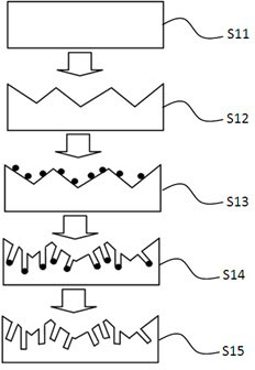
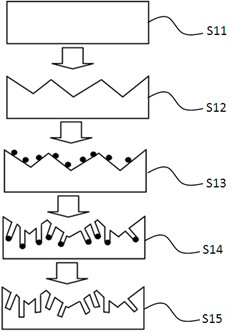
[0015] Embodiment 1: the monocrystalline silicon wafer is cleaned, and the alkaline etching solution is used for cashmere, forming a pyramid-shaped suede surface; then the silicon wafer is immersed in Na 2 S 2 o 8 and AgNO 3 In the aqueous solution, nanoscale silver particles are formed by chemical reduction and deposition on the surface of the silicon chip, and the particle size of the silver particles is 50nm; 2 o 2 and H 2 Selective etching in the chemical etching solution composed of O, HF: H 2 o 2 :H 2 The volume ratio of O is 1:(0.5~5):(5~20), preferably 1:5:20, the etching time is 3~10min, preferably 10min; finally put the silicon wafer into 50% concentrated HNO 3 solution to remove silver particles.

Embodiment 2

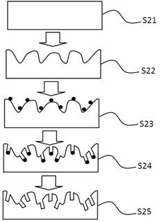
[0016] Example 2: Clean the single crystal silicon wafer, and make texture with alkaline corrosion solution to form a pyramid-shaped texture; then coat a layer of nano-gold particle emulsion wrapped by polymer on the surface of the silicon wafer, and the particle size of the gold particle is 5nm , dried; then put the silicon wafer covered with gold particles into 49% HF, 30% H 2 o 2 and H 2 Selective etching in the chemical etching solution composed of O, HF: H 2 o 2 :H 2 The volume ratio of O is 1:(0.5~5):(5~20), preferably 1:0.5:5; the etching time is 3~10min, preferably 3min; finally put the silicon wafer into the aqueous solution of KI and I2 to remove gold particles.

Embodiment 3

[0017] Embodiment 3: The monocrystalline silicon wafer is cleaned, and the alkaline corrosion solution is used to make texture to form a pyramid-like texture; then a layer of discontinuous nano-platinum particle layer is sputtered on the surface of the silicon wafer, and the particle size of the platinum particle is 30nm; then Put the silicon wafer covered with platinum particles into 49% HF and 30% H 2 o 2 and H 2 Selective etching in the chemical etching solution composed of O, HF: H 2 o 2 :H 2 The volume ratio of O is 1:(0.5~5):(5~20), preferably 1:3:10; the etching time is 3~10min, preferably 5min; finally put the silicon wafer into the aqua regia solution to clean and remove the platinum particles .


PUM

PropertyMeasurementUnit
particle diameteraaaaaaaaaa

Abstract

The invention relates to a method for preparing a crystalline silicon nanometer and micrometer composite texture surface. The method is technically characterized by comprising carrying out cleaning and texture surface making for a crystalline silicon wafer and forming a micrometer-scale texture surface; then uniformly covering a layer of discontinuous nanometer-scale precious metal particles on the surface of the silicon wafer; selectively corroding the surface of the silicon wafer by the aid of chemical corrosive liquid, and forming a nanometer-scale texture surface; and finally cleaning and removing the precious metal particles by the aid of chemical liquor. The composite texture surface prepared by the method has a micrometer-scale structure and a nanometer-scale structure, the structure of the texture surface is finer, a light trapping effect of the surface of the silicon wafer is greatly improved, short-circuit current of a battery can be effectively increased, and accordingly photoelectric conversion efficiency of the battery is enhanced.

Description

technical field [0001] The invention relates to a preparation method of crystalline silicon nanometer-micrometer composite suede. Background technique [0002] The focus of industrial scale production of crystalline silicon solar cells is to reduce cell production costs and improve cell efficiency. In terms of improving battery efficiency, reducing the reflection of light on the light-receiving surface of the battery and increasing the absorption of light by the battery is one of the effective means to improve battery efficiency. There are three main ways to increase the light absorption of the battery: one is to cover the surface of the battery with an anti-reflection film to reduce the reflection of light; the other is to grow a heterogeneous layer with a wide band gap on the surface of the battery to increase the spectral response range of light; Various suede surfaces are prepared on the surface of the battery to create a light trapping effect and reduce light reflectio...

Claims


Application Information

Patent Timeline
Patent Type & Authority Applications(China)
IPC IPC(8): H01L31/18
CPCY02P70/50
Inventor 杨雷何晨旭凌振江殷海亭王冬松王步峰
Owner REALFORCE POWER
Why Eureka
Try Eureka