Method for preparing cuprous oxide film

A technology of cuprous oxide and thin film, applied in the direction of final product manufacturing, sustainable manufacturing/processing, electrical components, etc., can solve the problems of low oxygen activity, poor crystal quality, and difficult precise control of the growth process, etc., to achieve optimal growth conditions , the effect of shortening the time

Inactive Publication Date: 2012-08-01
INST OF PHYSICS - CHINESE ACAD OF SCI
View PDF1 Cites 18 Cited by
  • Summary
  • Abstract
  • Description
  • Claims
  • Application Information

AI Technical Summary

Problems solved by technology

This method has the advantages of simple operation, low equipment requirements, and low preparation cost, but it takes a long time to oxidize the Cu film due to the low oxygen activity.
In addition, for thin film growth, the several preparation processes mentioned above have similar limitations, that is, the deposited thin fi...

Method used


Image

  • Method for preparing cuprous oxide film
  • Method for preparing cuprous oxide film
  • Method for preparing cuprous oxide film

Examples


Embodiment 1

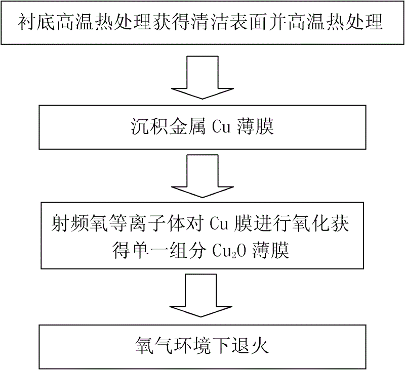
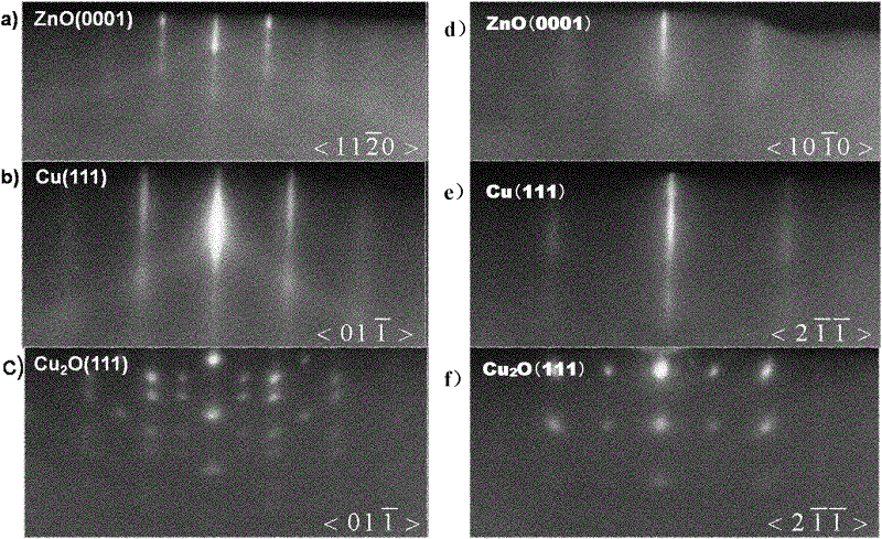
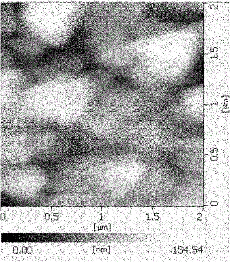
[0035] Embodiment 1 prepares high-quality Cu on ZnO single crystal substrate 2 O film

[0036] Such as figure 1 Shown process flow chart of the present invention, prepares high-quality Cu on zinc oxide single crystal substrate 2 The specific steps of O thin film are as follows:

[0037] 1) Remove the organic matter on the surface of the ZnO single crystal substrate by ultrasonic cleaning with acetone, alcohol, deionized water, etc., and then introduce the radio frequency plasma-assisted molecular beam epitaxy system (hereinafter referred to as the rf-MBE system);

[0038] 2) In an ultra-high vacuum environment, heat up to 750°C for 10 minutes of high-temperature heat treatment to remove surface-adsorbed inorganic impurities that cannot be removed by conventional cleaning;

[0039] 3) Perform radio frequency oxygen plasma treatment at the same temperature (750°C) for 10 minutes, the radio frequency power is 300W, and the oxygen flow rate is 2.0 sccm (cubic centimeters per mi...

Embodiment 2

[0048] Embodiment 2 prepares high-quality Cu on ZnO / sapphire (0001) single crystal substrate 2 O film

[0049] Such as figure 1 Shown process flow diagram of the present invention, prepares high-quality Cu on ZnO / sapphire (0001) single crystal substrate 2 The specific steps of O thin film are as follows:

[0050] 1) Plating molybdenum on the back of the commercially available sapphire substrate by magnetron sputtering, and ultrasonically cleaning with acetone, alcohol, and deionized water to remove organic matter on the substrate surface, and then introducing the substrate into the rf-MBE molecular beam epitaxy growth system ;

[0051] 2) deposit ZnO (0001) single crystal thin film on sapphire substrate with known method;

[0052] 3) The substrate is subjected to radio frequency oxygen plasma treatment at 500° C. for 10 minutes, with an oxygen flow rate of 2.0 sccm, to obtain a ZnO / sapphire (0001) template with an O-terminated surface;

[0053] 4) The substrate is heated ...

Embodiment 3

[0058] Example 3 on TiO 2 Preparation of High Quality Cu on Single Crystal Substrate 2 O film

[0059] Such as figure 1 Shown process flow diagram of the present invention, prepares high-quality Cu on titanium dioxide (rutile) single crystal substrate 2 The specific steps of O thin film are as follows:

[0060] 1) Plating molybdenum on the back of a commercially available rutile single crystal substrate by magnetron sputtering, and ultrasonically cleaning with acetone, alcohol, and deionized water to remove organic matter on the substrate surface, and then introducing the substrate into rf-MBE molecular beam epitaxy growth system;

[0061] 2) In an ultra-high vacuum environment, heat up to 900°C for 30 minutes of high-temperature heat treatment to remove impurities adsorbed on the surface;

[0062] 3) The substrate is cooled to 400° C., and subjected to radio frequency oxygen plasma treatment for 20 minutes. The radio frequency power is 340 W, and the oxygen flow rate is ...


PUM

PropertyMeasurementUnit
Resistivityaaaaaaaaaa
Mobilityaaaaaaaaaa

Abstract

The invention discloses a method for preparing a cuprous oxide film. The method comprises the following steps: step (1), selecting a monocrystal substrate and carrying out cleaning, and then introducing the cleaned monocrystal substrate into an ultrahigh vacuum film preparation system; step (2), carrying out heat treatment on the monocrystal substrate under the ultrahigh vacuum situation so as to remove surface impurities thereof; step (3), depositing a Cu film on the substrate surface processed in the step (2) under the condition that the air pressure is less than or equal to 10<-8>mbar, wherein the temperature of the substrate is in a range from 0 DEG C to 700 DEG C; step (4), carrying out oxidation treatment on the Cu film by utilizing radio frequency oxygen plasma; and step (5), carrying out annealing for 10 to 30 mins at the temperature of 600 to 900 DEG C and then reducing the temperature to a room temperature and taking the film out. According to the invention, growth of the Cu film with high quality is realized by utilizing an ultrahigh vacuum molecular beam epitaxial technology and a strong oxidizing property of an active oxygen atom. And the prepared Cu2O monocrystal film is expected to be applied in fields including a solar thin-film cell and an optoelectronic device and the like.

Description

technical field [0001] The present invention relates to a kind of preparation method of thin film, relate in particular to a kind of cuprous oxide (Cu 2 O) Preparation method of thin film. Background technique [0002] Cu 2 O is a direct bandgap oxide semiconductor material with a room temperature gap of 2.1eV and a free exciton binding energy of up to 140meV. It has a variety of superior photoelectric properties and is used in transparent conductive films, photocatalysis, photovoltaic devices and battery electrodes It is one of the earliest semiconductor materials for research and industrial application. [0003] Currently Cu 2 O thin film preparation processes mainly include thermal evaporation, sputtering, pulsed laser deposition, chemical vapor deposition, and electrochemical deposition. The common preparation method is to oxidize Cu film in an oxygen environment (usually an atmospheric pressure) to obtain Cu 2 O. This method has the advantages of simple operation,...

Claims


Application Information

Patent Timeline
IPC IPC(8): H01L31/032H01L31/18
CPCY02P70/50
Inventor 李俊强梅增霞叶大千崔秀芝杜小龙
Owner INST OF PHYSICS - CHINESE ACAD OF SCI
Why Eureka
Try Eureka