Silicon-based light emitting diode (LED) chip encapsulating method and LED chip luminous device

A technology of LED chips and packaging methods, which is applied in the direction of semiconductor devices, electrical components, circuits, etc., and can solve the effects of LED light-emitting devices on the luminous effect or effective light output, the effects of light-emitting device service life and work reliability, and increase the production cost of LED chips To achieve flexible and diverse product specifications, improve heat dissipation/heat conduction effect, luminous effect or effective light output improvement

Inactive Publication Date: 2012-08-01
SHANGHAI RES CENT OF ENG & TECH FOR SOLID STATE LIGHTING
View PDF6 Cites 2 Cited by
  • Summary
  • Abstract
  • Description
  • Claims
  • Application Information

AI Technical Summary

Problems solved by technology

[0008] 2. The current production line that adopts the flying wire method / wire bonding method to produce LED chips has a certain impact on the yield due to the problem of the gold wire connection pass rate, and the existence of the gold wire makes the service life and working reliability of the entire light emitting device are also affected to some extent;
[0009] 3. The gold wire spans above the LED chip, which hinders the light emitted by the LED chip, and has a certain impact on the luminous effect or effective light output of the LED light-emitting device;
[0010] 4. In the past two years, the price of gold has continued to rise, and the price of gold wire used for LED packaging has also continued to increase, which directly increases the production cost of LED chips
[0011] 5. The capacity of the existing production line for producing LED chips using the flying wire method / wire bonding method is close to saturation, but it is still far from meeting the actual market demand
[0014] If the existing integrated circuit IC chip packaging production line can be used to package LED chips, the production capacity of LED light-emitting devices can be greatly improved and the production cost can be reduced, which is beneficial to integrated circuit manufacturers and LED light-emitting device manufacturers / suppliers. It's a win-win thing

Method used


Image

  • Silicon-based light emitting diode (LED) chip encapsulating method and LED chip luminous device
  • Silicon-based light emitting diode (LED) chip encapsulating method and LED chip luminous device
  • Silicon-based light emitting diode (LED) chip encapsulating method and LED chip luminous device

Examples


Embodiment Construction

[0044] The present invention will be further described below in conjunction with the accompanying drawings.

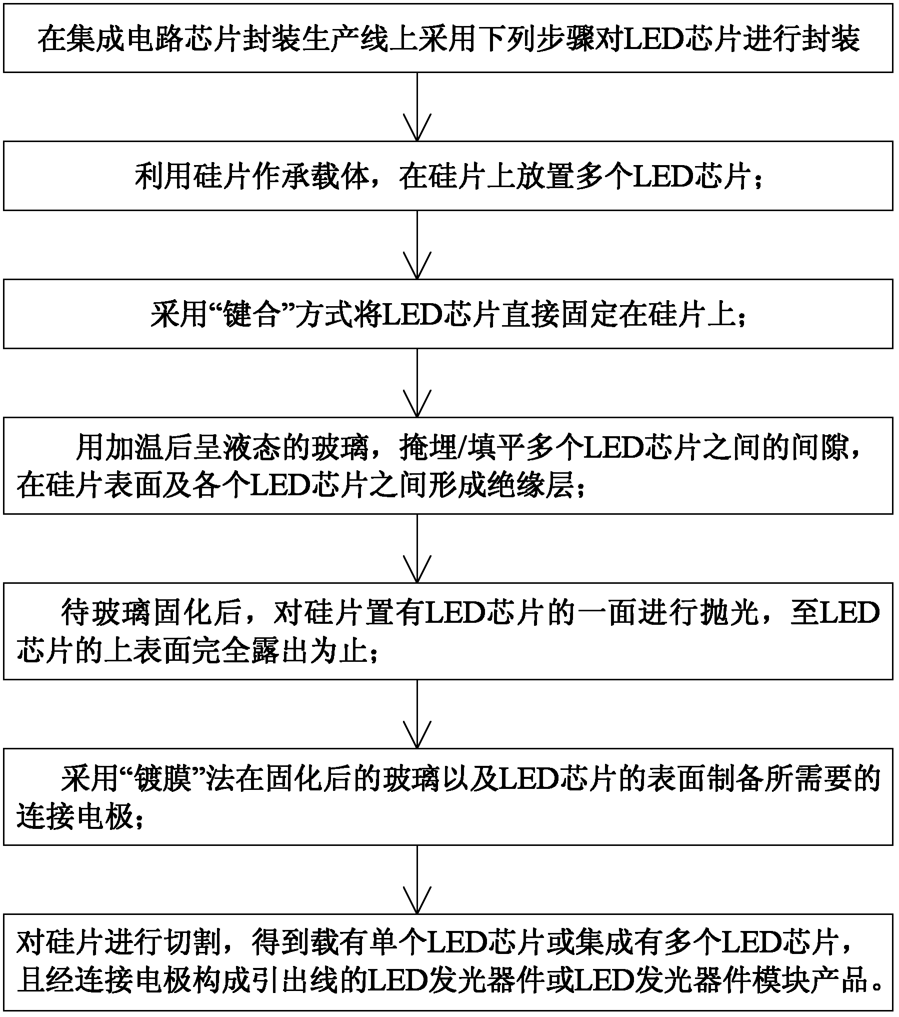
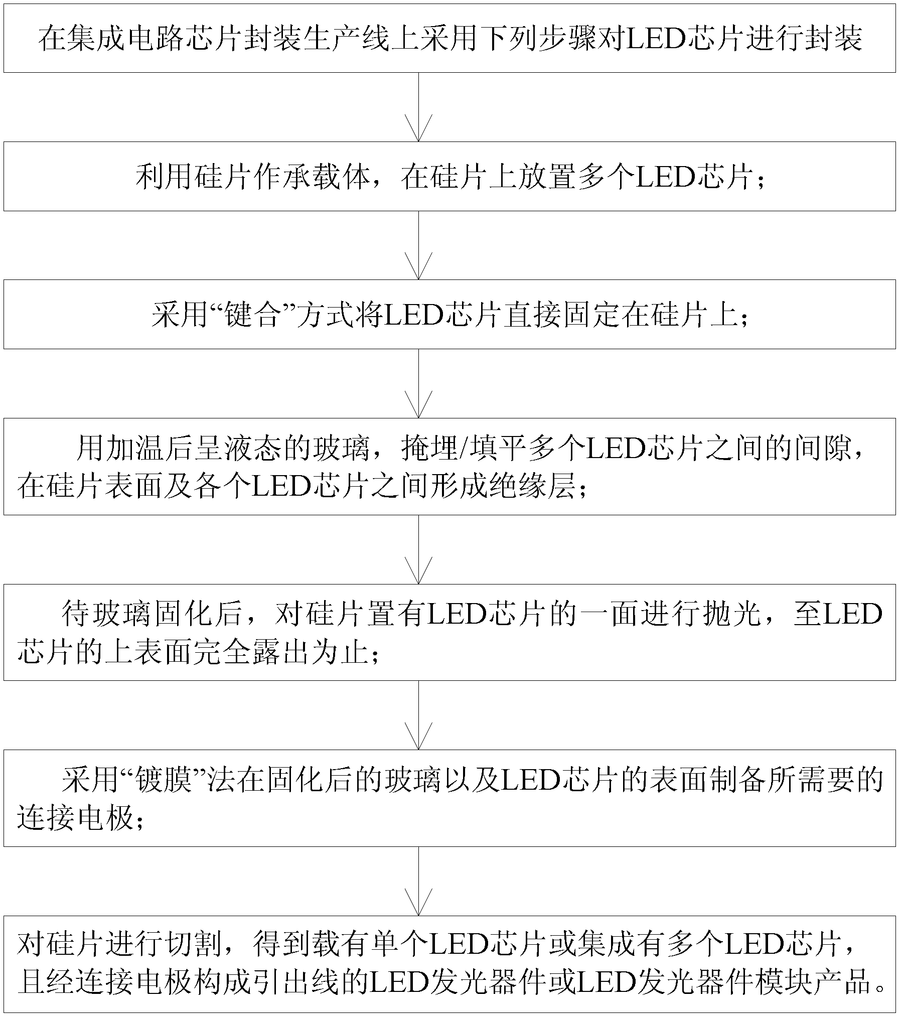
[0045] figure 1 Among them, this technical solution provides a silicon-based LED chip packaging method, which adopts the following steps to package the LED chip on the integrated circuit IC chip packaging production line:

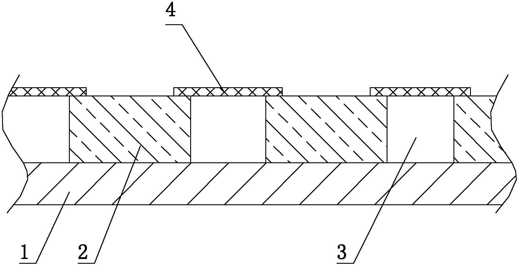
[0046] A. Using a silicon wafer as a carrier, place multiple LED chips on the silicon wafer;

[0047] B. Fix the LED chip directly on the silicon wafer by "bonding" method;

[0048] C. Use liquid glass after heating to bury / fill the gap between each LED chip, and form an insulating layer between the surface of the silicon wafer and each LED chip;

[0049] D. After the glass is solidified, polish the side of the silicon wafer with the LED chip until the LED chip is exposed;

[0050] E. Use the "coating" method to prepare the required connecting electrodes on the surface of the cured glass and the LED chip;

[0051] F. Cutting the silicon wafer to...


PUM


Abstract

The invention relates to a silicon-based light emitting diode (LED) chip encapsulating method and an LED chip luminous diode, and belongs to the field of a semiconductor device. An LED chip is encapsulated on an intelligent card (IC) chip encapsulation production line: a silicon sheet is used as a carrier, and the LED chip is directly and fixedly arranged on the silicon sheet in a bonding manner; insulation layers are respectively formed on the surface of the silicon sheet and among different LED chips by liquid glass; the surface of the silicon sheet which is provided with the LED chip is polished; connection electrodes are respectively prepared on the surfaces of the solidified glass and the LED chips through a film coating method; and the silicon sheet is cut to obtain the LED luminous device or an LED luminous device module product. Due to the adoption of the silicon-based LED chip encapsulating method and the LED chip luminous diode, the encapsulation cost of an LED is reduced, a brand new field is developed for the application and the use of the existing integrated circuit IC chip encapsulation production line, the method is particularly suitable for the production of the LED luminous device with larger power, and larger optical power can be outputted under the same external environmental condition or under the situation with the same power. The method can be widely applied to the production and manufacturing fields of the LED luminous device.

Description

technical field [0001] The invention belongs to the field of semiconductor devices, and in particular relates to a packaging method for LED chips and products thereof. Background technique [0002] With the increasingly widespread application of semiconductor lighting technology, the output of LED chips / light-emitting devices is growing rapidly. [0003] The structure of the existing LED light-emitting device is to bond the LED chip on a substrate, and then use the flying wire method / wire bonding method to lead the connecting wire (referred to as "gold wire" in the industry) from the P-N junction of the LED chip. Connect to the lead-out pin of the light-emitting device, and connect to the external power supply or circuit. [0004] "Gold wire", also known as ball bonding gold wire or lead wire, is an important material in the microelectronics industry, and is usually used as a connecting wire between a chip and a lead frame. [0005] The date of the authorization announceme...

Claims


Application Information

Patent Timeline
Patent Type & Authority Applications(China)
IPC IPC(8): H01L33/48H01L33/62H01L33/64
Inventor 李抒智马可军
Owner SHANGHAI RES CENT OF ENG & TECH FOR SOLID STATE LIGHTING
Why Eureka
Try Eureka