Method and apparatus for manufacturing IGBT device

A device and silicon wafer technology, applied in the field of electronic devices, can solve the problems of low activation rate of N-type and P-type impurities, insufficient elimination of defects, uneven annealing, etc., and achieve the effect of flexible and changeable implementation modes.

Inactive Publication Date: 2012-09-26
上海永电电子科技有限公司
View PDF6 Cites 27 Cited by
  • Summary
  • Abstract
  • Description
  • Claims
  • Application Information

AI Technical Summary

Problems solved by technology

[0006] First, after ion implantation of FS and impurities required for the collector, the annealing temperature should not be too high (generally less than 450°C), otherwise it will affect the characteristics of the MOSFET device 05 that has been made on the front side. The low annealing temperature makes N-type and P-type The impurity activation rate is low, and the defects generated by ion implantation cannot be fully eliminated, resulting in large IGBT leakage
Laser annealing can ma

Method used


Image

  • Method and apparatus for manufacturing IGBT device
  • Method and apparatus for manufacturing IGBT device
  • Method and apparatus for manufacturing IGBT device

Examples


Embodiment Construction

[0035] In the following description, many technical details are proposed in order to enable readers to better understand the application. However, those skilled in the art can understand that without these technical details and various changes and modifications based on the following implementation modes, the technical solution claimed in each claim of the present application can also be realized.

[0036] In order to make the purpose, technical solution and advantages of the present invention clearer, the following will further describe the implementation of the present invention in detail in conjunction with the accompanying drawings.

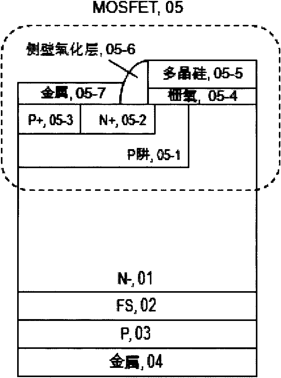
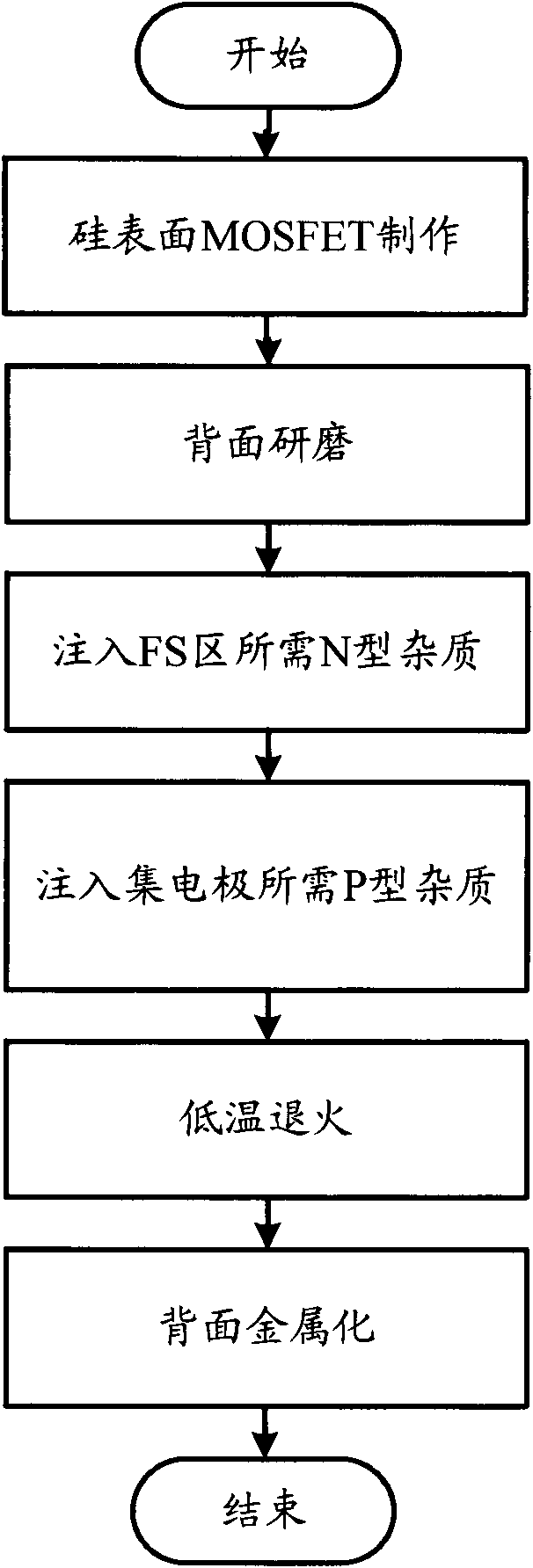
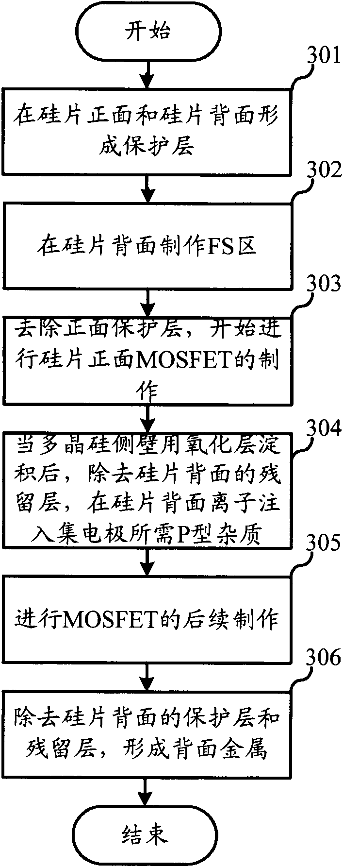
[0037] The first embodiment of the present invention relates to a method for manufacturing an IGBT device, the specific process is as follows image 3 shown.

[0038]In step 301, a protection layer is formed on the front side and the back side of the silicon wafer. Specifically, N-type silicon wafers are selected first, and the N-doping con...


PUM


Abstract

The invention, which relates to the electronic device field, discloses a method and apparatus for manufacturing an insulated gate bipolar transistor (IGBT) device. According to the invention, forming of a field stop (FS) region and a collector at a back side of an IGBT device is not carried out after completion of a metal-oxide-semiconductor field effect transistor (MOSFET) manufacturing of the IGBT and back-side grinding but is carried out before, after and during the MOSFET manufacturing process in an interspersed mode. A thick FS is formed; after the forming of the FS with the needed thickness, devices like a front-side MOSFET are manufactured without influencing characteristics of devices that are manufactured afterwards and includes a MOSFET at a front side of a silicon ship. And the high temperature process of the manufacturing of the devices at the front-side of the silicon chip has little impact on the FS with the thickness of 20 to 30 micrometers. Ion implantation of P type impurities of the back-side collector is carried out after deposition of an oxide layer at the side wall of the front-side MOSFET and the activation of the P type impurities is carried out by the thermal process of the manufacturing of the front side MOSFET; and the activation rate is high and the damage caused by the ion implantation can be eliminated. Therefore, an IGBT with high breakdown voltage, low electricity leakage, conduction voltage drop positive temperature coefficient and low switching loss is manufactured.

Description

technical field [0001] The invention relates to the field of electronic devices, in particular to the IGBT device manufacturing technology in the field of electronic devices. Background technique [0002] Insulated gate bipolar transistor (Insulated Gate Bipolar Transistor, referred to as "IGBT") technology has developed rapidly in recent years, and has become one of the most important high-power mainstream devices in the field of power electronics. The earliest types of IGBTs include punch through ("PT" for short) and non-punch through ("NPT" for short). In recent years, field stop (Field stop, referred to as "FS") structure IGBT has been developed, in which the FS region is an N-type doped region, which is higher in doping concentration than the N-region in the IGBT. The rapid reduction achieves electric field termination. The conduction voltage drop or conduction loss of the FS type IGBT is low, and the temperature coefficient of the conduction voltage drop is positive,...

Claims


Application Information

Patent Timeline
IPC IPC(8): H01L21/331H01L21/28
CPCH01L29/36H01L29/7395H01L29/66333
Inventor 高文玉马正焜邹世昌
Owner 上海永电电子科技有限公司
Why Eureka
Try Eureka