
Novel Low-Voltage High-Performance Non-volatile Memory Based on Discrete Nanographene Floating Gate

A nano-graphene and memory technology, which is applied in the direction of electric solid-state devices, semiconductor devices, electrical components, etc., can solve the problems of unrealizable size, high-temperature annealing, and expensive metal nanocrystals, so as to optimize charge distribution and retention characteristics , optimize the storage charge distribution and capacity, and realize the effect of high-performance operation

Active Publication Date: 2016-03-09
INST OF PHYSICS - CHINESE ACAD OF SCI
View PDF4 Cites 1 Cited by
  • Summary
  • Abstract
  • Description
  • Claims
  • Application Information

AI Technical Summary

Problems solved by technology

However, the floating gate memories of these nanocrystalline materials also face many problems in the process of scaling down. For example, the quantum confinement effect of semiconductor nanocrystals leads to a decrease in charge storage capacity when scaled down; metal nanocrystals are expensive and many preparation technologies It is not compatible with the CMOS process, and cannot achieve uniform and controllable size. It is easy to diffuse or undergo chemical reactions during high-temperature annealing, and cannot achieve high-density device integration when the scale is reduced. The chemical stability of metal-organic nanocrystals is poor, and high-temperature annealing is not possible. Poor retention characteristics; oxide nanocrystals cannot reduce power consumption, charge storage capacity is weak, etc.

Method used


Image

  • Novel Low-Voltage High-Performance Non-volatile Memory Based on Discrete Nanographene Floating Gate
  • Novel Low-Voltage High-Performance Non-volatile Memory Based on Discrete Nanographene Floating Gate
  • Novel Low-Voltage High-Performance Non-volatile Memory Based on Discrete Nanographene Floating Gate

Examples


Embodiment Construction

[0026] In order to make the object, technical solution and advantages of the present invention clearer, the present invention will be further described in detail in conjunction with specific embodiments and with reference to the accompanying drawings.

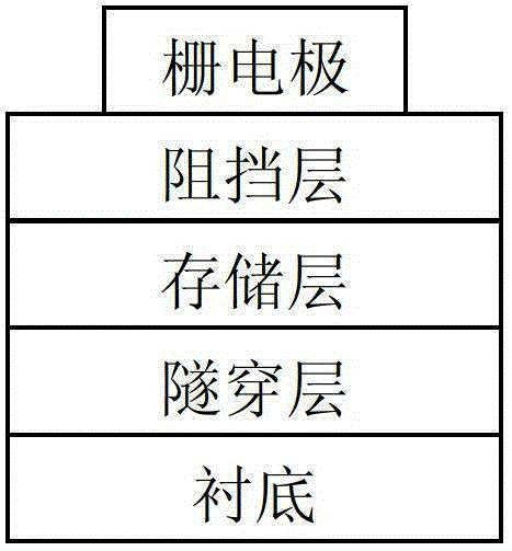
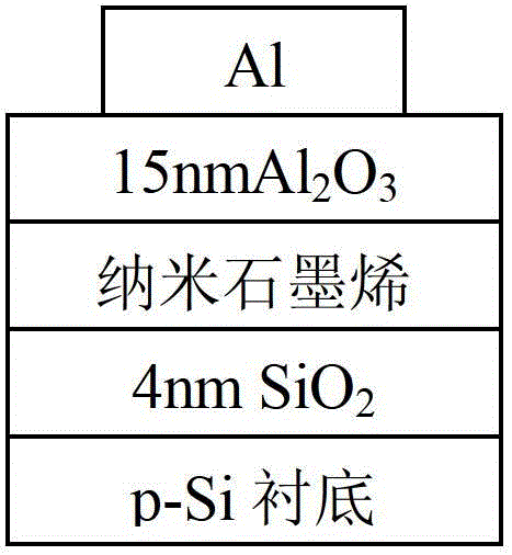
[0027] figure 1 It is a schematic diagram of the cell structure of the nano-graphene floating gate non-volatile memory of the present invention. The structure of the present invention includes a substrate, a tunneling layer, a storage layer, a blocking layer and a gate electrode. The tunneling layer and barrier layer can use wide bandgap dielectric materials such as SiO 2 、Al 2 o 3 , HfO 2 , or other materials with similar properties. The thickness of each thin layer can be adjusted according to the different materials used. The storage layer is composed of nano-graphene floating gates, and the main storage function is nano-graphene and the interface between nano-graphene and the dielectric layer. The surface morphology ...


PUM


Abstract

The invention discloses a novel low-voltage high-performance nonvolatile memory based on a separate nano graphene floating gate. The novel low-voltage high-performance nonvolatile memory comprises a substrate, a tunneling layer, a storage layer, a barrier layer and a gate electrode, wherein the storage layer is of separate nano graphene, and by utilizing the density and size modulating action of the nano graphene and the energy band modulating action of the tunneling layer, the charge distribution and holding characteristic of the storage layer can be optimized. By introducing the separate nano graphene floating gate, a nonvolatile flash memory with low energy consumption under low-voltage operation can be realized; and by effectively controlling the density and size of the nano graphene and modulating the energy band structure of the tunneling oxidizing layer, the charge distribution and holding characteristic of the storage layer can be optimized, and the high-performance operation of devices can be realized.

Description

technical field [0001] The invention relates to a floating gate type nonvolatile storage device, in particular to a novel discrete nano-graphene floating gate nonvolatile storage device with low voltage and high performance, and belongs to the technical field of nanomaterial manufacturing and storage. Background technique [0002] In the electronic information age, non-volatile memory, as one of the most important integrated circuit products, has a wide range of applications and an irreplaceable position in the fields of computers, multimedia applications, mobile network communications, consumer electronics, and defense electronic equipment. Especially its mainstream product - flash memory with the advantages of fast programming speed, high density, low power consumption, small size and high reliability, has occupied most of the market of non-volatile memory. [0003] However, with the continuous improvement of market demand and the continuous development of process technolo...

Claims


Application Information

Patent Timeline
Patent Type & Authority Patents(China)
IPC IPC(8): H01L27/115H01L29/792H01L29/49
Inventor 张广宇杨蓉时东霞
Owner INST OF PHYSICS - CHINESE ACAD OF SCI
Learn More