Micro-nano structured D-shaped optical fiber, method for producing same and application
A micro-nano structure and optical fiber technology, applied in the field of optoelectronics, can solve the problems of complex mask manufacturing process, difficult to realize complex pattern preparation, high cost, and achieve good repeatability, simple and efficient preparation scheme, and guarantee resolution and transfer accuracy. Effect
- Summary
- Abstract
- Description
- Claims
- Application Information
AI Technical Summary
Problems solved by technology
Method used
Image

Examples
Embodiment 1
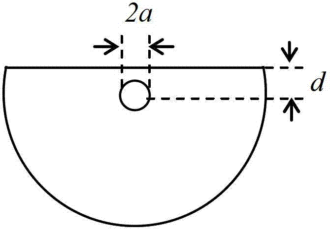
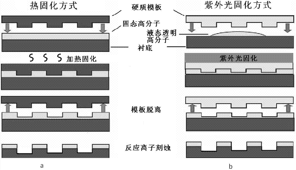
[0035] On the quartz substrate, a regular concave-convex pattern (a period of 2.5um, a two-dimensional ball array with a diameter of 1um, and a depth of 300nm) was constructed by photolithography. Reactive ion etching transferred the structure to the substrate, and oxygen plasma was applied to the surface of the quartz structure. Body treatment (etching 5s), followed by anti-sticking treatment. Add supporting fixtures on both sides of the D-shaped optical fiber, and make it flat with the plane of the D-shaped optical fiber, and then spin-coat a layer of UV-curable adhesive (mr-NIL6000 from Micro resist company, rotating speed 3000r / min, time 1min, Thickness about 500nm). Press the structured side of the quartz template down onto the plane of the D-shaped optical fiber, apply a pressure of 15 bar under nitrogen protection, keep it for 60 seconds, and then turn on the UV lamp at a rate of 50 mW / cm 2 Irradiate with high power for 5 minutes to fully cure the UV glue. After remov...
Embodiment 2
[0038] On the silicon nitride substrate template, a regular concave-convex pattern (a two-dimensional grid array with a period of 7um, a line width of 500nm, and a depth of 200nm) was constructed by photolithography. Reactive ion etching transferred the structure to the substrate, and the surface of the substrate was After treatment (oxygen plasma etching for 5s), anti-sticking treatment is performed. Then PDMS (Silicone elastomer KIT 184, Daw corning, KIT 184 silicone rubber, Dow Corning Company) was spin-coated on the substrate with the structure carved (spin-coating speed 600r / min, time 12s, film thickness about 300nm), vacuum degassing After 30min, it was cured at 60°C for 5h. Lightly brush a layer of UV curing glue (OG154 UV glue from EPO-TEK company, thickness about 400nm) on the plane of the D-shaped optical fiber, peel off the cured PDMS from the silicon nitride substrate, with the structured side facing down , attached to the D-shaped optical fiber plane, so that the...
Embodiment 3
[0041] A layer of polymethyl methacrylate PMMA (thickness about 500nm) was spin-coated on the single crystal silicon substrate template, and a regular concave-convex pattern (period 700nm, line width 350nm) was constructed by E-beam lithography One-dimensional grating array, depth 300nm), reactive ion etching to transfer the structure to the substrate, after surface treatment of the substrate (oxygen plasma etching for 5s), anti-sticking treatment. Then PDMS was spin-coated on the substrate with the structure (spin-coating speed 600r / min, film thickness about 300nm), vacuum degassed for 30min and cured at 60°C for 5h. Lightly brush a layer of PMMA on the D-shaped optical fiber plane, peel off the cured PDMS from the single crystal silicon substrate, and stick it on the D-shaped optical fiber plane with the structured side facing down. ) to make the two fully contact, raise the temperature to 160°C and keep it for 6min, then start to cool down to 80°C, remove the PDMS, and reac...
PUM
| Property | Measurement | Unit |
|---|---|---|
| depth | aaaaa | aaaaa |
| thickness | aaaaa | aaaaa |
| width | aaaaa | aaaaa |
Abstract
Description
Claims
Application Information
 - Generate Ideas
- Intellectual Property
- Life Sciences
- Materials
- Tech Scout
- Unparalleled Data Quality
- Higher Quality Content
- 60% Fewer Hallucinations
Browse by: Latest US Patents, China's latest patents, Technical Efficacy Thesaurus, Application Domain, Technology Topic, Popular Technical Reports.
© 2025 PatSnap. All rights reserved.Legal|Privacy policy|Modern Slavery Act Transparency Statement|Sitemap|About US| Contact US: help@patsnap.com