

Graphene mode-locked optically pumped thin disc semiconductor laser
A semiconductor and graphene technology, applied in the field of graphene mode-locked optically pumped thin-film semiconductor lasers, achieves the effects of short saturable recovery time, simple structure, and narrow output pulse width
- Summary
- Abstract
- Description
- Claims
- Application Information
AI Technical Summary
Problems solved by technology
Method used
Image

Examples
Embodiment 1
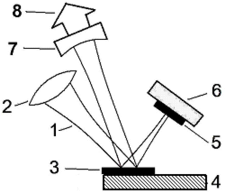
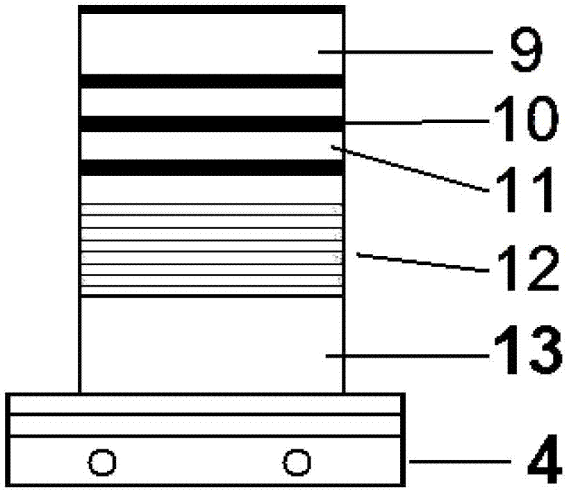
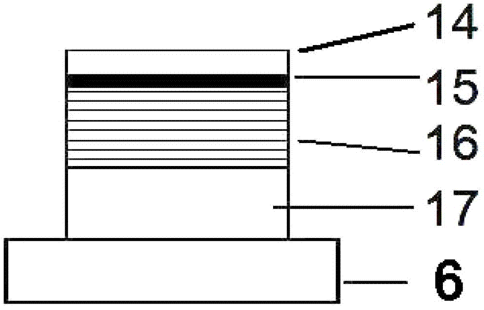
[0026] For the output pulsed light wavelength is the laser near 1 micron, the pump light source 1 is the semiconductor laser with the optical fiber output of 800-810nm wavelength; In the semiconductor gain chip 3, the semiconductor quantum well active layer 10 in the periodic quantum well layer is InGaAs, wherein the In content is 0.18-0.20, the quantum well barrier layer 11 in the periodic multi-quantum well layer is GaAs or AlGaAs, and the number of quantum wells is 6-16; the semiconductor Bragg mirror layer 12 is 26-28 For GaAs / AlAs. The semiconductor gain chip 3 uses a heat sink 4 to remove excess heat and control the chip temperature. The schematic diagram of the structure of the cooling device 4 is as Figure 4 As shown, the semiconductor gain chip is pasted on the heat sink 18 with heat-conducting glue, and the heat sink is copper or pure copper; the heat sink 18 is connected to the semiconductor refrigerator 19 with In to control the chip temperature; the semiconducto...
Embodiment 2
[0028] It is 630-670nm semiconductor laser that the pump light source in embodiment 1 is changed into wavelength, the periodic multi-quantum well layer is changed into GaAs / AlGaAs quantum well and potential barrier, and graphene saturable absorption mirror is changed into the absorption of carbon nanotube material The mirror can obtain the mode-locked pulse light output near 850nm.
Embodiment 3
[0030] It is the semiconductor laser of 808nm that the pumping light source among the embodiment 1 is changed into, the periodic multi-quantum well layer is changed into GaInNAs / GaAs quantum well and potential barrier, and the graphene saturable absorbing mirror is changed into the carbon nanotube material absorbing mirror, Then the mode-locked pulse light output near 1220nm can be obtained.
PUM
 Abstract
Description
Claims
Application Information