Preparation method for FS-IGBT device

A device and semiconductor technology, applied in the field of power semiconductor devices, can solve problems such as high annealing temperature, easy oscillation, and influence on device reliability, so as to ensure the integrity of silicon wafers, reduce equipment requirements, and excellent device performance. Effect

Inactive Publication Date: 2012-11-28
UNIV OF ELECTRONICS SCI & TECH OF CHINA +1
View PDF5 Cites 40 Cited by
  • Summary
  • Abstract
  • Description
  • Claims
  • Application Information

AI Technical Summary

Problems solved by technology

However, this increases the difficulty of the process. At present, the FS layer is usually introduced by doing the front side process first, and then injecting the back sheet. Since the metal pattern on the front side needs to be protected, the annealing temperature should not be too high. At this time, the impurity activation rate is very low, which affects Device performance
Some manufacturers use laser annealing to solve this problem. Although this advanced process technology can solve the problem of low impurity activation rate, it cannot advance the impurity, and due to the limitation of wavelength, the annealing depth is limited. A thinner FS layer is obtained at the back collector area. This FS layer cannot maximize the withstand voltage level of the device. In addition, the thinner FS layer will affect the reliability of the device, and it is easy to generate oscillation when it is turned off.

Method used


Image

  • Preparation method for FS-IGBT device
  • Preparation method for FS-IGBT device
  • Preparation method for FS-IGBT device

Examples


Embodiment Construction

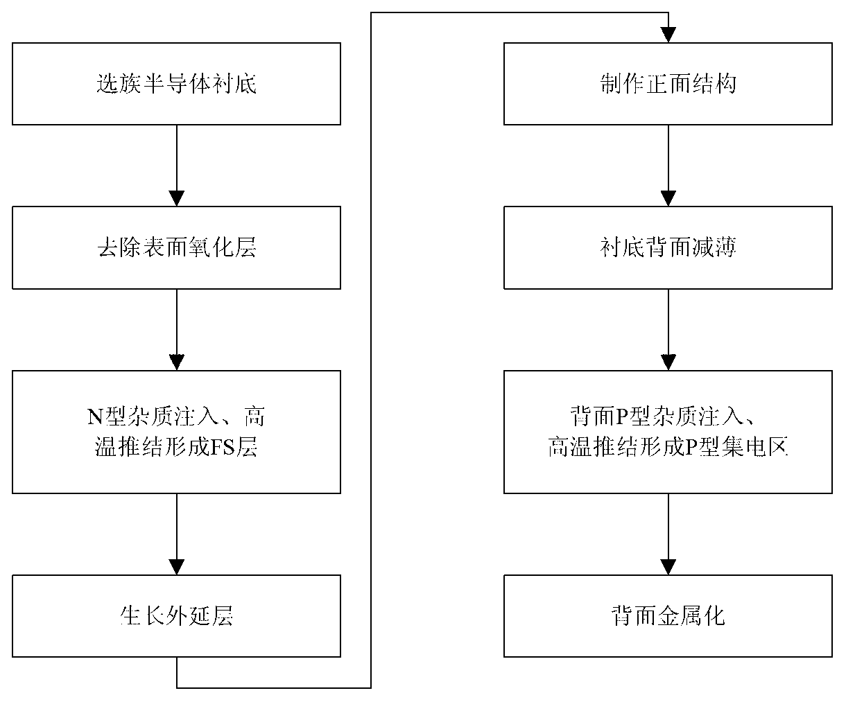
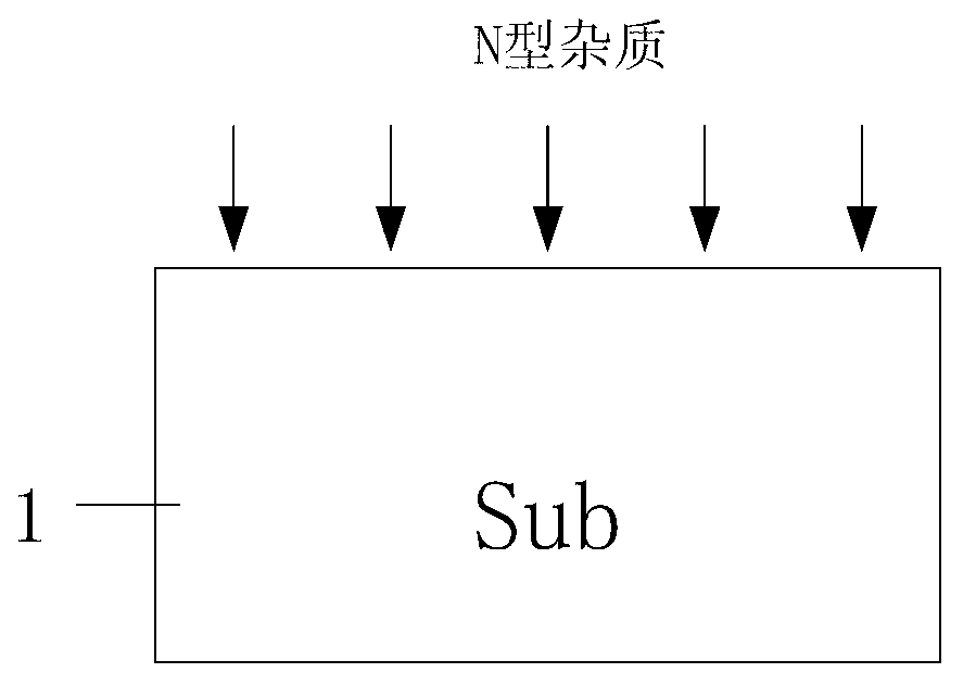
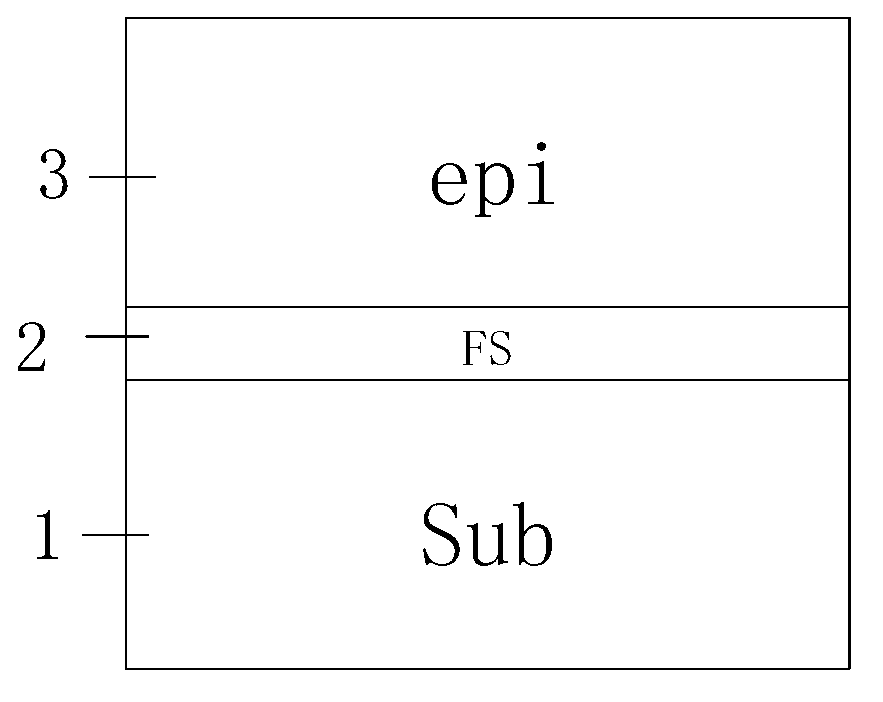
[0032] A method for manufacturing a power device, taking a trench field stop type insulated gate bipolar transistor as an example, includes selecting a silicon wafer, removing a surface oxide layer, injecting N-type impurities and pushing the junction at high temperature to form an FS layer, growing an epitaxial layer, growing Field oxide layer, lithography active area and field limiting ring terminal, grow scattering oxide layer and inject boron, etch away scattering oxide layer and anneal push junction, photolithography emitter area, grow scattering oxide layer and implant N-type impurities, remove Scatter the oxide layer and anneal and push the junction, remove the oxide layer and deposit silicon nitride, photolithography the groove area and etch the Trench groove, grow the gate oxide layer, fill the polycrystalline, etch part of the polycrystalline and planarize, and oxidize the polycrystalline area And remove silicon nitride, deposit passivation layer, perform ohmic contac...


PUM


Abstract

A preparation method for an FS-IGBT (Field Stop-Insulated-Gate Bipolar Transistor) device belongs to the technical field of power semiconductor devices. In the preparation method, N-type impurity injection is performed on a substrate to form a field stop layer, then an epitaxial layer is generated, a front patterning is manufactured, then the back part is thinned, injection and annealing for a P-type collector region on the back part are performed, a manner of metalization on the back part is adopted to manufacture a field stop transistor, and impurities in the field stop layer can be activated fully. In addition, the preparation method can lead in an N-type transition region between the field stop layer and the P-type collector region by controlling thermal budget and back thinning positions, and the performance of the device can be improved.

Description

technical field [0001] The invention belongs to the technical field of power semiconductor devices, and relates to an insulated gate bipolar transistor (IGBT), especially a preparation method of a field stop type insulated gate bipolar transistor (FS-IGBT). Background technique [0002] Power semiconductor technology is the core of power electronics technology. With the development of microelectronics technology, modern power semiconductor technology represented by gate-controlled power devices has developed rapidly since the 1980s, which has greatly promoted the progress of power electronics technology. [0003] The power MOS tube is a voltage-controlled device, which can control the switching of the device by controlling the gate voltage. The structure of the driving circuit is simple, and the single-carrier conductivity makes it excellent in switching characteristics. However, multisub devices cannot produce conductance modulation effects in the drift region, so they are ...

Claims


Application Information

Patent Timeline
Patent Type & Authority Applications(China)
IPC IPC(8): H01L21/331
Inventor 李泽宏杨文韬单亚东夏小军李长安张蒙张金平任敏张波
Owner UNIV OF ELECTRONICS SCI & TECH OF CHINA
Why Eureka
Try Eureka