Large-scale integrated interconnection electromigration failure test method

A large-scale integrated interconnection and large-scale integration technology, applied in the field of testing, can solve the problems of high test cost, inability to obtain time information, low test efficiency, etc., and achieve the effect of improving test efficiency, reducing test time and reducing test cost.

Inactive Publication Date: 2012-12-19
XIDIAN UNIV
View PDF4 Cites 6 Cited by
  • Summary
  • Abstract
  • Description
  • Claims
  • Application Information

AI Technical Summary

Problems solved by technology

[0003] Existing research on electromigration failure of integrated circuit interconnection generally uses single-link structure interconnection for failure experiments, and the test efficiency is very low. In order to reduce the test cycle, multiple test devices are often required to work at the same time, and the test cost is high; The method of building an external bypass circuit with diodes realizes the electromigration failure test of series structure mul

Method used


Image

  • Large-scale integrated interconnection electromigration failure test method
  • Large-scale integrated interconnection electromigration failure test method
  • Large-scale integrated interconnection electromigration failure test method

Examples


Embodiment 1

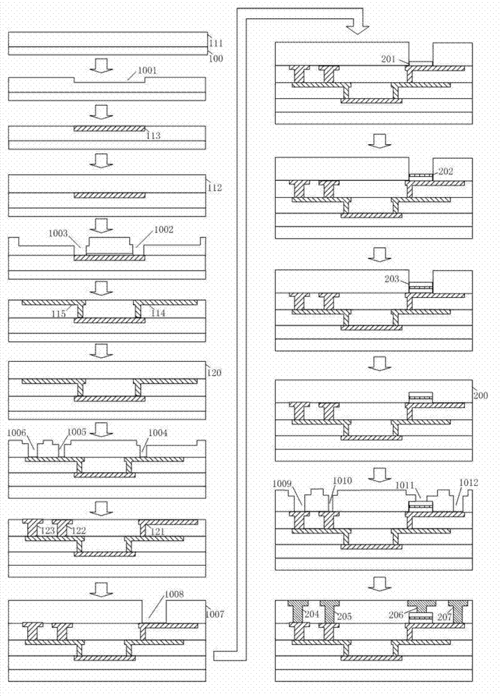
[0058] Such as figure 2 The material of the interconnection-antifuse unit shown is copper. The length of the first-level interconnection line 113 is 300 micrometers. The upper metal electrode 203 and the lower metal electrode 201 of the antifuse are made of titanium nitride with a thickness of 200 nanometers, and the material of the intermediate insulating medium 202 is silicon nitride with a thickness of 5 nanometers.

Embodiment 2

[0060] Such as figure 2 The material of the interconnection-antifuse unit shown is aluminum. The length of the first-level interconnection line 113 is 350 micrometers. The material of the upper metal electrode 203 and the lower metal electrode 201 of the antifuse is titanium tungsten with a thickness of 250 nanometers, and the material of the intermediate insulating medium 202 is amorphous silicon with a thickness of 60 nanometers.

Embodiment 3

[0062] Such as figure 2 The material of the interconnection-antifuse unit shown is copper. The length of the first-level interconnection line 113 is 400 micrometers. The material of the upper metal electrode 203 and the lower metal electrode 201 of the antifuse is titanium nitride with a thickness of 300 nanometers, and the material of the intermediate insulating medium 202 is a hydrogen-containing amorphous carbon film doped with nitrogen and fluorine elements with a thickness of 25 nm. Nano.

[0063] The performance of the present invention can be specified by the following tests.


PUM

PropertyMeasurementUnit
Thicknessaaaaaaaaaa
Thicknessaaaaaaaaaa
Thicknessaaaaaaaaaa

Abstract

The invention discloses a large-scale integrated interconnection electromigration failure test method, mainly to solve the problems of high test cost and small test scale in the prior art. The large-scale integrated interconnection electromigration failure test method adopts the following technical scheme: an antifuse is formed on a welding plate of an integrated interconnection line through a plane integration process by using the characteristic that a resistor has a great change before and after the antifuse is programmed, interconnection and antifuse parallel structures are formed, a large amount of the interconnection and antifuse unit structures are connected in series to form a large-scale integrated interconnection multilink structure, and a test current source and a voltage meter are connected to the two ends of the multilink structure respectively and used for testing electromigration failure and recording voltage drop jump point time at the two ends of the multilink structure as interconnection failure time. The large-scale integrated interconnection electromigration failure test method has the advantages of low test cost and high test efficiency, and can be applied to testing large-scale integrated interconnection electromigration failure.

Description

technical field [0001] The invention belongs to the technical field of testing, and relates to reliability testing of semiconductor devices, in particular to a testing method for electromigration failure of large-scale integrated interconnection. Background technique [0002] With the continuous reduction of the feature size of integrated circuit devices and the increase of circuit complexity, the interconnection density, the number of layers and the working current density continue to increase, and the problem of electromigration failure of the interconnection caused by this is also more significant. One of the main failure phenomena is also one of the important contents of integrated circuit reliability evaluation. [0003] Existing research on electromigration failure of integrated circuit interconnection generally uses single-link structure interconnection for failure experiments, and the test efficiency is very low. In order to reduce the test cycle, multiple test devic...

Claims


Application Information

Patent Timeline
IPC IPC(8): G01R31/26
Inventor 吴振宇杨银堂陈雪薇
Owner XIDIAN UNIV
Why Eureka
Try Eureka