Method for realizing submicron-level process line width in manufacturing of silicon carbide power electronic devices

A power electronic device, sub-micron technology, applied in semiconductor/solid-state device manufacturing, electrical components, circuits, etc., can solve problems such as large on-resistance, affecting device performance, material damage, etc., to achieve low cost and simple process. Effect

Inactive Publication Date: 2012-12-19
DONGGUAN TIANYU SEMICON TECH
View PDF3 Cites 2 Cited by
  • Summary
  • Abstract
  • Description
  • Claims
  • Application Information

AI Technical Summary

Problems solved by technology

Traditional Si-based MOSFETs often cannot be used in the high-power field due to their large on-resistance at higher voltages
[0003] Since the current commercial silicon carbide wafers are mostly 4 inches, it is difficult to achieve a sub-micron process line width in the ultraviolet exposure lithography process on the 4-inch microelectronics process line, and the electron beam exposure lithography process has a significant impact on the surface of the material. Damaged, affecting device performance
The purchase of advanced lithography equipment requires a large investment, which cannot meet actual needs

Method used


Image

  • Method for realizing submicron-level process line width in manufacturing of silicon carbide power electronic devices

Examples


Embodiment 1

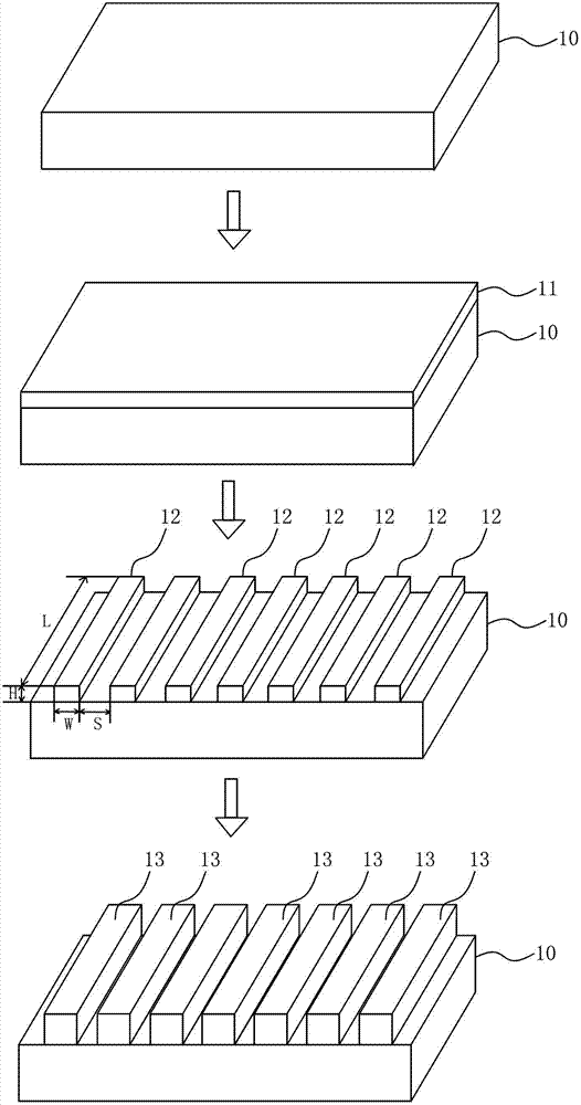
[0025] The material of the silicon carbide semiconductor thin film 10 is an N-type 4H-SiC (0001) 8° wafer with a thickness of 390 μm and a doping concentration of 1×10 16 cm -3 , wherein, the silicon carbide semiconductor thin film 10 needs to be cleaned by standard RCA, and RCA is the most commonly used wet chemical cleaning method.

[0026] The method for growing the silicon thin film layer 11 is a plasma-enhanced chemical vapor deposition method, wherein the crystal form of the silicon thin film layer 11 is polysilicon, and the thickness of the silicon thin film layer 11 is 0.7 μm.

[0027] The photolithography technique is a dry etching technique, the silicon thin film patterns 12 are in the shape of parallel strips, the etching width S between the silicon thin film patterns 12 is 2 μm, and the etching depth H is 0.7 μm. The width W of the portion is 2 μm, and the length L of the unetched portion thereof is 5 μm.

[0028] To oxidize the sample, put the sample into a tubu...

Embodiment 2

[0030] This embodiment is similar to the above-mentioned embodiment 1, except that the oxidation temperature of this embodiment is 1300° C., the oxidation time is 250 minutes, and the thickness of the oxide layer is about 1.5 μm. After the silicon thin film pattern 12 is oxidized, the width of each side is widened to 0.8 μm, so that the gap between the silicon oxide thin film 13 after the silicon thin film pattern 12 is oxidized becomes 0.4 μm.


PUM

PropertyMeasurementUnit
Thicknessaaaaaaaaaa
Thicknessaaaaaaaaaa
Widthaaaaaaaaaa

Abstract

The invention discloses a method for realizing a submicron-level process line width in manufacturing of silicon carbide power electronic devices. The method comprises the following steps of: a, taking a silicon carbide semiconductor film; b, growing a silicon thin film layer on the silicon carbide semiconductor film; c, obtaining a silicon thin film pattern on the silicon thin film layer by using a photoetching technology; and d, carrying out oxidation on a sample, and through controlling the oxidation time, enabling multiple separated silicon thin films to be expanded to the two sides thereof, so that after the two sides of the silicon thin film pattern are widened to a certain value, a silicon oxide thin film with a submicron line width is formed and can be used as a mask layer in manufacturing of silicon carbide power electronic devices. According to the invention, through controlling the conditions such as oxidation temperature and time and the like, the width of the silicon thin film subjected to oxidation can be accurately controlled to be increased by 0.01-10mu m, so that a gap between silicon oxide thin films can be accurately controlled to 0.1mu m even a smaller magnitude, thereby realizing the submicron-level process line width in manufacturing of silicon carbide power electronic devices.

Description

Technical field: [0001] The invention relates to the technical field of semiconductors, in particular to a method for realizing submicron process line width in the manufacture of silicon carbide power electronic devices. Background technique: [0002] Silicon carbide (SiC) is an important wide-bandgap semiconductor material, which has great application potential in the fields of high-temperature, high-frequency and high-power devices. Compared with traditional silicon (Si) materials, SiC has obvious advantages, for example, its forbidden band width is 3 times that of Si, the saturation electron drift rate is 2.5 times that of Si, and the breakdown electric field is 10 times that of Si. In addition to the above advantages, SiC is the only compound semiconductor that can form its own oxide (SiO 2 ) compound semiconductors, while SiO 2 It is the most commonly used insulating dielectric material in the semiconductor device preparation process, so SiC material can be compatible...

Claims


Application Information

Patent Timeline
IPC IPC(8): H01L21/04H01L21/02
Inventor 何志郑柳刘胜北黄亚军樊中朝季安杨富华孙国胜李锡光
Owner DONGGUAN TIANYU SEMICON TECH
Why Eureka
Try Eureka