Source-field-plate heterojunction field-effect transistor and manufacturing method thereof

A heterojunction field effect and source field plate technology, applied in the fields of semiconductor/solid-state device manufacturing, semiconductor devices, electrical components, etc., can solve the complex manufacturing process of heterojunction field effect transistors, the reduction of device yield and uniformity, Can not completely shield the gate-drain capacitance and other problems, to achieve the effect of high yield, improved power gain characteristics, and easy implementation

Inactive Publication Date: 2013-01-16
XIDIAN UNIV
View PDF2 Cites 15 Cited by
  • Summary
  • Abstract
  • Description
  • Claims
  • Application Information

AI Technical Summary

Problems solved by technology

However, due to the relatively long distance between the source field plate and the gate field plate, even if the source field plate structure is used, it still cannot completely shield the gate-drain capacitance and obtain the best power gain characteristics.
At the same time, the manufacturing process of heterojunction field effect transistors with a multilayer field plate structure has

Method used


Image

  • Source-field-plate heterojunction field-effect transistor and manufacturing method thereof
  • Source-field-plate heterojunction field-effect transistor and manufacturing method thereof
  • Source-field-plate heterojunction field-effect transistor and manufacturing method thereof

Examples


Embodiment 1

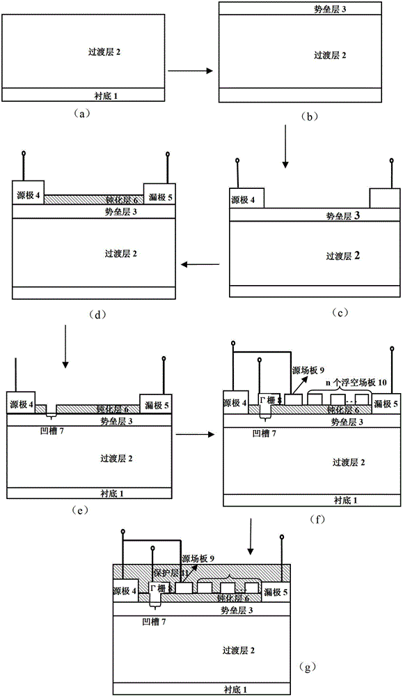
[0052] Embodiment 1: Made on a SiC substrate, the passivation layer medium is SiN, the protective layer is SiN, the Γ grid, the source field plate and the floating metal field plate are metal stacks composed of Ni and Au from bottom to top A source field plate heterojunction field effect transistor, the steps of which include the following:

[0053] The first step is to grow 100nm AlN at 1050°C on the SiC substrate using metal organic chemical vapor deposition technology MOCVD, and then grow a 1μm unintentionally doped GaN layer at 1000°C to form a buffer layer 2 .

[0054] In the second step, a barrier layer 3 with a thickness of 27 nm is deposited on the buffer layer 2 by metal organic chemical vapor deposition technique MOCVD. The barrier layer is composed of 1.2nm thick AlN, 25nm thick AlGaN layer with 27% Al composition and 0.8nm GaN layer from bottom to top. The temperature of layer AlGaN is 1110°C, and the temperature of deposition of top layer GaN is 1110°C.

[0055...

Embodiment 2

[0068] Embodiment 2: making passivation layer medium on sapphire substrate is Al 2 o 3 , the protective layer is AlN, the Γ gate, the source field plate and the floating metal field plate are a source field plate heterojunction field effect transistor composed of metal stacks composed of Pt and Au from bottom to top.

[0069] The production steps of this example are as follows:

[0070] Step A, on the sapphire substrate, use metal organic chemical vapor deposition technology MOCVD, first grow 100nm AlN at 1050°C, and then grow 2.5μm unintentionally doped AlGaN layer at 1000°C, Al composition 10 %, forming a buffer layer (2).

[0071] In step B, a barrier layer 3 with a thickness of 27 nm is deposited on the buffer layer 2 by metal organic chemical vapor deposition technique MOCVD. The barrier layer is composed of 1.2nm-thick AlN, 25nm-thick AlGaN layer with Al composition of 40% and 0.8nm GaN layer from bottom to top. The temperature of the AlGaN layer is 1110°C, and the t...

Embodiment 3

[0079] Embodiment 3: Making a passivation layer medium on a GaN substrate is HfO 2 , the protective layer is SiO 2 , The Γ gate, the source field plate and the floating metal field plate are source field plate heterojunction field effect transistors composed of Ni, Au and Ni metal stacks from bottom to top.

[0080] The steps in this example are as follows:

[0081] Step 1: On the GaN substrate, use metal organic chemical vapor deposition technology MOCVD to grow 100nm AlN at 1050°C, and then grow a 4μm unintentionally doped GaN layer at 1000°C to form a buffer layer 2 .

[0082] In the second step, a barrier layer 3 with a thickness of 9 nm is deposited on the buffer layer 2 by metal organic chemical vapor deposition technique MOCVD.

[0083] The barrier layer is 1nm thick AlN and 8nm thick InAlN layer with 83% Al composition from bottom to top; the temperature for growing the AlN layer is 1000°C, and the temperature for growing the top layer InAlN is 750°C.

[0084] The ...


PUM

PropertyMeasurementUnit
Thicknessaaaaaaaaaa
Thicknessaaaaaaaaaa
Thicknessaaaaaaaaaa

Abstract

The invention discloses a source-field-plate heterojunction field-effect transistor and a manufacturing method, and mainly solves the problems of low breakdown voltage and low power gain in the conventional field-plate technology. The source-field-plate heterojunction field-effect transistor comprises a substrate (1), a transition layer (2), a potential barrier layer (3), a source electrode (4), a drain electrode (5), a passivating layer (6), a Gamma-shaped grid (8) and a protective layer (11), wherein the passivating layer (6) is provided with a groove (7); a part of the Gamma-shaped grid (8) is positioned in the groove (7), and the other part of the Gamma-shaped grid (8) is positioned at the upper part of the passivating layer (6); the passivating layer (6) between the Gamma-shaped grid (8) and the drain electrode (5) is provided with a source field plate (9) and n floating metal field plates (10); the source field plate (9) is connected with the source electrode (4); the floating metal field plates are same in length, and the distances among the field plates are same; and the Gamma-shaped grid (8), the source field plate (9) and the n floating metal field plates (10) are manufactured by using a same metal deposition process so as to form the source-field-plate heterojunction field-effect transistor. The source-field-plate heterojunction field-effect transistor and the method have the advantages of high breakdown voltage, little grid-drain feedback capacitance, high power grain and simpleness for process, and is applicable to high-frequency and large-power III-V compound microwave power devices.

Description

technical field [0001] The invention belongs to the field of microelectronics, relates to semiconductor devices, and can be used in the fields of microwave power amplifiers, wireless radars, single-chip integrated circuits and the like. Background technique [0002] As the third-generation semiconductor material, GaN material shows great potential in the fields of high frequency, high temperature, high voltage and high power due to its large band gap, high critical breakdown field strength, high carrier mobility and saturation velocity. Great advantage. Since 1993, Khan et al. reported the successful development of the first AlGaN / GaN heterojunction high electron mobility transistor. After continuous improvement in material quality, device technology and device structure, its performance has continuously made breakthroughs. However, there are still many problems in AlGaN / GaN microwave power devices that have not been resolved. The two key problems are the phenomenon of larg...

Claims


Application Information

Patent Timeline
IPC IPC(8): H01L29/778H01L29/423H01L21/335
Inventor 郝跃张凯马晓华陈永和曹梦逸
Owner XIDIAN UNIV
Why Eureka
Try Eureka