Electrically erasable programmable read only memory (EEPROM) storage chip especial for intelligent ammeter

A technology of smart energy meter and storage chip, applied in the field of microelectronics, can solve the problems of large chip area, high size, high cost and system complexity, and high production cost, so as to reduce the device size and chip area, and save the number of manufacturing masks. , the effect of low cost

Inactive Publication Date: 2013-02-20
BEIJING TIANZHONGLEI INTELLIGENT TECH
View PDF4 Cites 2 Cited by
  • Summary
  • Abstract
  • Description
  • Claims
  • Application Information

AI Technical Summary

Problems solved by technology

[0005] The technical problem to be solved by the present invention is to provide a dedicated EEPROM memory chip for smart energy meters, which can solve the problem of large chip area and the need for a large number of masks due to the use of floating gate memory structures such as MNOS, SONOS, and polysilicon in existing memory chips. Problems such as covering chips and high production costs; and solving the problems of high size, cost and system complexity caused by the use of general-purpose memory chips in existing smart energy meters

Method used


Image

  • Electrically erasable programmable read only memory (EEPROM) storage chip especial for intelligent ammeter
  • Electrically erasable programmable read only memory (EEPROM) storage chip especial for intelligent ammeter
  • Electrically erasable programmable read only memory (EEPROM) storage chip especial for intelligent ammeter

Examples


no. 1 example

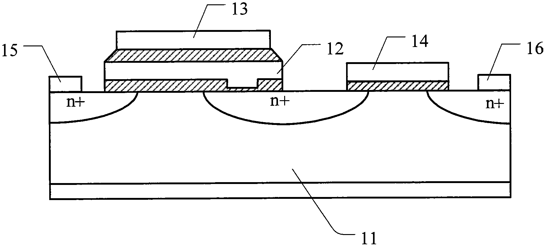
[0027] In this preferred embodiment, the core storage unit of the dedicated EEPROM memory chip for smart electric energy meters is a 1T storage unit composed of a single planar floating gate nanocrystalline memory transistor, and a high-density storage array is formed based on the 1T storage unit; The structure of the EEPROM can be used, or Nor Flash or its improved structure (such as DiNOR, DuSNOR, etc.), can also be designed according to the application scenario needs (such as specific chip specifications, capacity and other related parameters) to design a specific structure, as long as it can Ensure that each memory cell (single bit) in the memory array can be flexibly addressed, programmed, erased and other operations; the write mode of the memory cell selects the FN tunneling method or the channel hot electron injection method (such as CHEI , SSI, etc.); the erasing method of the memory cell selects the FN tunneling method or the hot hole band band tunneling injection (BBHH...

no. 2 example

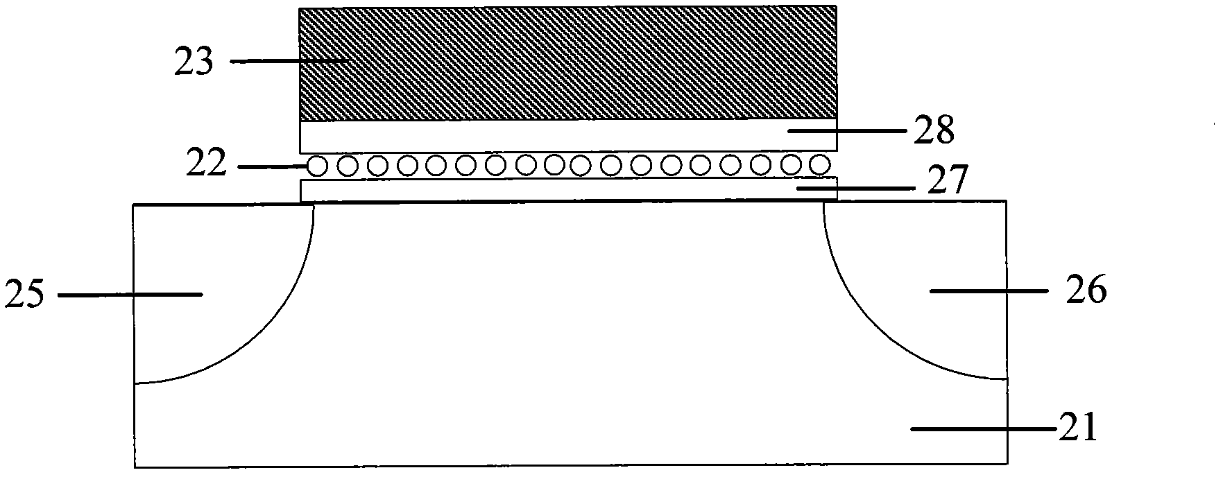
[0034] In this preferred embodiment, the nanocrystalline memory cell of the dedicated EEPROM memory chip for smart energy meters is a 1.5T memory cell composed of nanocrystalline memory transistors with a split gate structure, and a high-density memory array is formed based on the 1.5T memory cell. Reference image 3 , Shows a schematic diagram of the nanocrystalline memory cell structure of the second embodiment of the EEPROM memory chip dedicated for smart energy meters of the present invention, including: Si substrate material 31; N+ formed by heavily doping the N-type substrate region of the substrate material 31 The source conductive region 35 and the N+ drain conductive region 36; the select gate dielectric layer 39 covering the channel surface and located under the transistor select gate 34; the tunneling dielectric layer 37 covering the channel surface and located under the transistor control gate 33; transistor The nanocrystalline storage layer 32 below and on the side ...

no. 3 example

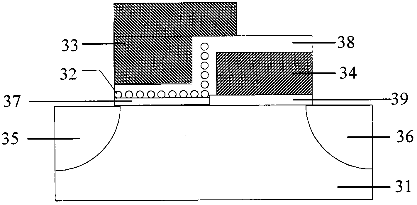
[0039] In this preferred embodiment, the core storage unit of the dedicated EEPROM memory chip for smart energy meters is a 2T storage unit formed by a single planar floating gate nanocrystalline storage transistor and a selection transistor in series, and a high-density storage unit is formed based on the 2T storage unit Storage array. Reference Figure 4-3 , Shows a schematic diagram of the nanocrystalline memory cell structure of the third embodiment of the EEPROM memory chip dedicated for smart energy meters of the present invention, including: a semiconductor substrate material 41, a source conductive region formed by heavily doping the substrate area of ​​the substrate material 41 45 and the first drain conductive region 46-1, the second drain conductive region 46-2, the tunneling dielectric layer 47 covering the carrier channel between the source conductive region 45 and the first drain conductive region 46-1, tunneling The nanocrystalline memory layer 42 covered on the ...


PUM


Abstract

The invention provides an electrically erasable programmable read only memory (EEPROM) storage chip especial for an intelligent ammeter. The EEPROM storage chip comprises a storage array which is composed of nanocrystalline storage units, wherein each of the nanocrystalline storage units comprises a semiconductor substrate material, a source conduction region, a leak conduction region, a tunneling dielectric layer, a nanocrystalline storage layer, an isolation dielectric layer and a transistor control grid, the source conduction region and the leak conduction region are formed by heavy doping in a substrate region of the semiconductor substrate material, the tunneling dielectric layer is covered on the surface of a channel between the source conduction region and the leak conduction region, the nanocrystalline storage layer is covered on the tunneling dielectric layer, the tunneling dielectric layer encircles or covers the nanocrystalline storage layer, the transistor control grid is covered on the isolation dielectric layer, and the storage array utilizes a framework which is capable of performing random addressing, programming and erasing to each storage unit in the array. Nanocrystalline floating gate storage structures are used as the storage units, so that manufacturing processes can be simplified, device sizes and chip areas are lessened, the number of masks to be manufactured is reduced, and manufacturing costs of the storage chip are reduced.

Description

Technical field [0001] The present invention relates to the technical field of microelectronics, in particular to a special EEPROM storage chip for smart electric energy meters. Background technique [0002] With the increasing popularity of electronic devices, semiconductor memory technology has developed rapidly in recent years. Semiconductor memory can be divided into two types: volatile and non-volatile. Among them, non-volatile semiconductor memory represented by EEPROM and Flash has been widely used in many fields such as communications, aerospace, and power grids. Taking the power grid field as an example, with the deepening of the national smart grid construction, the overall market demand for storage chips has become larger and larger. In addition, the design life of smart meters is generally 8 to 10 years, and it is generally replaced after 5 years of use. Market demand It also has a strong continuity. [0003] The memory chips currently on the market are generally gene...

Claims


Application Information

Patent Timeline
Patent Type & Authority Applications(China)
IPC IPC(8): H01L27/115G11C16/06
Inventor 刘璟谢伟东李天石田漪婷
Owner BEIJING TIANZHONGLEI INTELLIGENT TECH
Why Eureka
Try Eureka