Nano-gold surface-enhanced Raman active substrate with layered three-dimensional structure and method for preparing same

A surface-enhanced Raman, three-dimensional structure technology, applied in Raman scattering, microstructure technology, microstructure devices, etc., can solve the problems of poor signal uniformity, complex preparation process, low sensitivity, etc., and achieve strong Raman signal and detection. Sensitive and inexpensive effects

Inactive Publication Date: 2013-02-27
JIANGXI NORMAL UNIV
View PDF5 Cites 14 Cited by
  • Summary
  • Abstract
  • Description
  • Claims
  • Application Information

AI Technical Summary

Problems solved by technology

[0004] The purpose of the present invention is to provide a layered three-dimensional structure nano-gold surface-enhanced Raman active substrate and its preparation method to solv

Method used


Image

  • Nano-gold surface-enhanced Raman active substrate with layered three-dimensional structure and method for preparing same
  • Nano-gold surface-enhanced Raman active substrate with layered three-dimensional structure and method for preparing same
  • Nano-gold surface-enhanced Raman active substrate with layered three-dimensional structure and method for preparing same

Examples


Embodiment 1

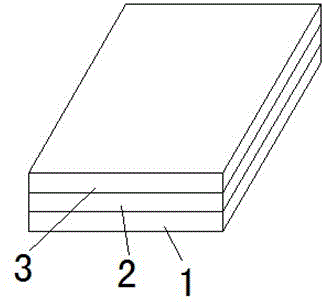
[0029] Such as figure 1 As shown, the layered three-dimensional structure nano-gold surface-enhanced Raman active substrate in this embodiment consists of a gold film (1), a silicon dioxide dielectric layer (2) and a two-dimensional gold nano-particle array (3) in sequence from bottom to top. composition. In this embodiment, the schematic diagram of the preparation of the layered three-dimensional structure nano-gold surface-enhanced Raman active substrate is as follows figure 1 shown. In this embodiment, the surface-enhanced Raman active substrate of nano-gold with a layered three-dimensional structure can be widely used in the analysis and detection of low-concentration organic molecules and biomolecules.

Embodiment 2

[0031] This embodiment adopts two materials of gold and silicon dioxide. First, a gold film with a thickness of 100 nm is deposited on the glass slide by ion beam coating; secondly, ion beam coating is used on the gold film substrate. Methods A silicon dioxide dielectric film with a thickness of 40 nm was deposited; finally, a two-dimensional gold nanoparticle array was directly deposited on the gold film-dielectric film by ion beam coating. The difference between this embodiment and specific embodiment example 1 is that the average particle diameter of nano gold particles in the surface-enhanced Raman active substrate of layered three-dimensional gold nanostructure is 5-70 nm, and other parameters are the same as specific embodiment example 1.

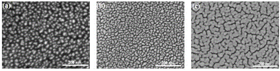
[0032] In this embodiment, the obtained two-dimensional gold nanoparticle array (3) of the layered three-dimensional structure nano-gold surface-enhanced Raman active substrate is characterized by surface microscopic morphology, as sho...

Embodiment 3

[0034] The difference between this embodiment and the specific embodiment 1 or 2 is that the thickness of the intermediate medium layer (2) of the surface-enhanced Raman active substrate of the layered three-dimensional gold nanostructure is 20-60 nm, and other parameters are the same as those of the specific embodiment 1 or 2. .

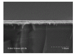
[0035] In this embodiment, the side microscopic morphology of the three-dimensional structure of the obtained layered three-dimensional structure gold nano surface enhanced Raman active substrate is characterized, as image 3 shown. Depend on image 3 It can be seen that the structure has an obvious three-layer structure, and the thickness is uniform.


PUM

PropertyMeasurementUnit
Thicknessaaaaaaaaaa
Thicknessaaaaaaaaaa
Particle sizeaaaaaaaaaa

Abstract

A nano-gold surface-enhanced Raman active substrate with a layered three-dimensional structure and a method for preparing the same relate to the fields of the nanometer materials science, laser Raman and biochemical analysis and detection. The surface-enhanced Raman active substrate is composed of three layers in total: a gold film, a dielectric layer and a two-dimensional array of irregular nano-gold particles arranged orderly from the bottom upwards, wherein the size and shape of the nano-gold particles and the thickness of each layer are adjustable. The method for preparing the substrate provided by the invention is to deposit the layered three-dimensional structure on a commercial glass slide with gold and silicon dioxide as coating materials by the ion beam coating method without using any other method. The nano-gold surface-enhanced Raman active substrate with the layered three-dimensional structure solves the problems of poor signal, low sensitivity, complex preparation process, high cost and the like of the nano-gold surface-enhanced Raman active substrate prepared by the prior art, and can be used for analyzing and detecting low-content compounds.

Description

technical field [0001] The invention relates to a layered three-dimensional structure nano-gold surface enhanced Raman active substrate and a preparation method thereof. Background technique [0002] Since the discovery of the Raman effect in 1927, Raman spectroscopy has been widely used in the fields of physics, biology, chemistry, and medicine due to its real-time, non-destructive, and rapid detection characteristics. However, due to the low Raman scattering efficiency and weak signal, it is difficult for ordinary Raman spectroscopy to monitor trace substances and single-molecule behaviors (such as conformational changes, mutual recognition, interaction, etc.) in real time. In 1974, Fleischaman et al. discovered that adsorption of pyridine on the rough surface of a silver electrode can obtain enhanced Raman signals, which is Surface-enhanced Raman scattering (Surface-enhanced Raman scattering, referred to as SERS). Since surface-enhanced Raman scattering can greatly i...

Claims


Application Information

Patent Timeline
IPC IPC(8): G01N21/65B81C1/00
Inventor 刘桂强刘正奇黎磊陈元浩黄宽胡莹张向楠唐发林龚丽霞
Owner JIANGXI NORMAL UNIV
Why Eureka
Try Eureka