Manufacturing method of MOS (metal oxide semiconductor) device of integrated Schottky diode

A technology for Schottky diodes and MOS devices, which is applied in semiconductor/solid-state device manufacturing, electrical solid-state devices, semiconductor devices, etc., can solve problems such as increasing process complexity, reduce process complexity, improve utilization, and device design. flexible effects

Active Publication Date: 2013-02-27
SHANGHAI INTEGRATED CIRCUIT RES & DEV CENT
View PDF5 Cites 11 Cited by
  • Summary
  • Abstract
  • Description
  • Claims
  • Application Information

AI Technical Summary

Problems solved by technology

[0003] In U.S. Patent No. 7,816,732, a method of integrating trench MOSFET and Schottky diode into the same chip is disclosed, by depositing a layer of oxide on the surface of the device, dry oxide etching and dry silicon etching etch to form anode contact holes, gate contact holes and source-body contact trenches, and then deposit barrier layers, metal tungsten and chemical mechanical polishing in the anode contact holes, gate contact holes and source-body contact trenches. Forming trench source-body contact regions, planar anode contact regions and planar gate contact regions, this method undoubtedly increases the process complexity

Method used


Image

  • Manufacturing method of MOS (metal oxide semiconductor) device of integrated Schottky diode
  • Manufacturing method of MOS (metal oxide semiconductor) device of integrated Schottky diode
  • Manufacturing method of MOS (metal oxide semiconductor) device of integrated Schottky diode

Examples


Embodiment Construction

[0019] In order to make the content of the present invention clearer and easier to understand, the content of the present invention will be further described below with reference to the accompanying drawings. Of course, the present invention is not limited to this specific embodiment, and general substitutions known to those skilled in the art are also covered within the protection scope of the present invention.

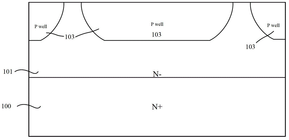
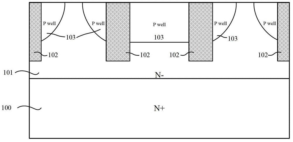
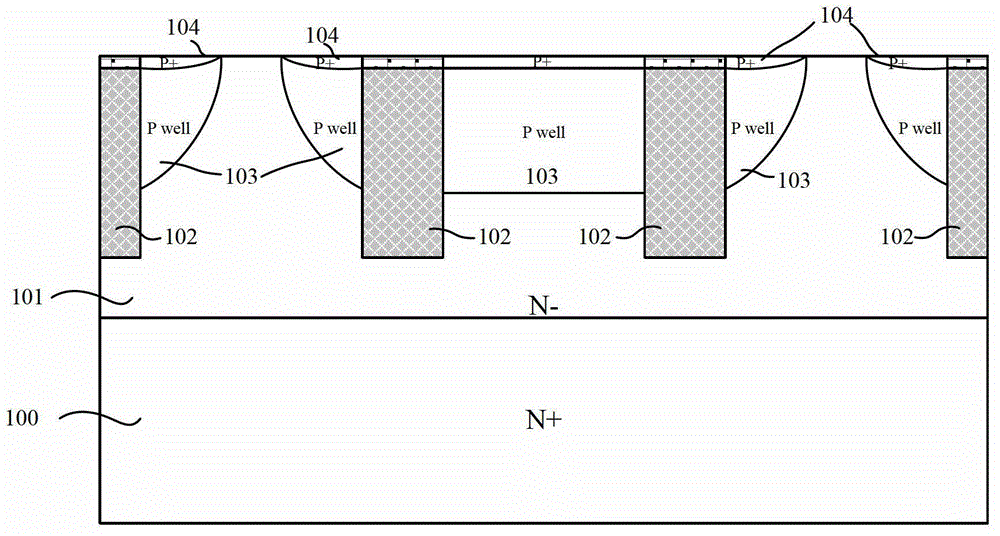
[0020] Figure 1 to Figure 5 Shown is a method of fabricating a Schottky diode-integrated MOS device according to an exemplary embodiment of the present invention. In the following description of the embodiment, descriptions of well-known steps, processes, materials, dopants, etc. are omitted. Furthermore, those skilled in the art will appreciate that the steps described below can be performed in a different order and are not limited to the examples set forth below. Those skilled in the art should also understand that "+" and "-" are used below to describe the rela...


PUM


Abstract

The invention discloses a manufacturing method of an MOS (metal oxide semiconductor) device of an integrated Schottky diode. The manufacturing method comprises the following steps: providing a first conductive type of semiconductor substrate; forming a first conductive type of epitaxial layer on the substrate; carrying out ion implantation and diffusion of a second conductive type of doping agent on the epitaxial layer to form a plurality of second conductive type of regions, wherein preset interval regions are formed among the regions; forming a plurality of groove grids, second conductive type of contact regions and first conductive type of source regions in each region; depositing and etching an interlayer dielectric layer to ensure that the interlayer dielectric layer covers the groove grids and partial source regions to form contact holes; and depositing a metal layer on the contact holes, wherein the metal layer and the epitaxial layer of the preset interval regions form the Schottky diode. Through the adoption of the manufacturing method, the Schottky diode can be directly formed on the surface of the substrate without silicon etching, and the process complexity can be reduced.

Description

technical field [0001] The invention relates to the field of semiconductor integrated circuits, in particular to a method for manufacturing a MOS device integrating Schottky diodes. Background technique [0002] With the development of semiconductor technology and device technology, the breakdown voltage of trench MOSFET devices (UMOSFET) can easily reach hundreds of volts, far exceeding conventional MOSFET devices. At the same time, due to the voltage control of the MOSFET device itself and the faster turn-off speed of the bipolar device, the power MOSFET device is widely used in the application field of high-speed switching power supply management with an operating voltage below 200V. For example, in a DC / DC circuit, two power MOSFETs are usually used in series, and the two power MOSFET devices are controlled by two gate control signals to turn on and off respectively, so as to transmit power to the load. In the DC / DC circuit, in order to avoid the shoot-through current f...

Claims


Application Information

Patent Timeline
Patent Type & Authority Applications(China)
IPC IPC(8): H01L21/336H01L21/329H01L27/06H01L29/872H01L29/78
Inventor 周伟全冯溪
Owner SHANGHAI INTEGRATED CIRCUIT RES & DEV CENT
Why Eureka
Try Eureka