A kind of manufacturing method of microfluidic chip mold
A technology of microfluidic chip and manufacturing method, which is applied in the direction of replication/marking method, microstructure technology, microstructure device, etc., which can solve the problems of expensive equipment processing accuracy, low structure surface flatness, long mold production cycle, etc., to achieve The effect of good flatness, shortened processing flow and time, and convenient mass production
- Summary
- Abstract
- Description
- Claims
- Application Information
AI Technical Summary
Problems solved by technology
Method used
Image
Examples
Embodiment 1
[0029] Example 1. Use a laser printer to print coated paper, and use the glycerin soaking method to make a microfluidic chip mold
[0030] Such as figure 1 As shown, the chip pattern is first printed on the coated paper using a laser printer. The area with ink on the coated paper will exhibit hydrophobic properties, while the blank area without ink (that is, the chip pattern) will exhibit hydrophilic properties. Cut the coated paper into a suitable size and immerse it in glycerin, then pick it up slowly to realize the separation of glycerin and coated paper, and then the glycerin will remain in the chip pattern area without ink, (for the convenience of observation, blue dye is added to the glycerin ). The glycerol adhered to the chip pattern will shrink due to surface tension to form a smooth arc-shaped convex structure, that is, the microfluidic chip mold is obtained.
Embodiment 2
[0031] Example 2, using a laser printer to print coated paper, using glycerin to smear and then centrifuging or gas blowing to make a microfluidic chip mold
[0032] The printing of pattern is the same as embodiment 1. Such as figure 2 As shown, a layer of glycerin will be formed by spraying or smearing on the printed coated paper, and then it will be centrifuged in a centrifuge or blown with nitrogen. If the force is small, the glycerin will be thrown away, and the glycerin will be attached to the place where there is no ink, forming the convex structure required for the mold of the microfluidic chip.
Embodiment 3
[0033] Embodiment 3, use the method of the present invention to make the PDMS chip layer that contains dimple and pipeline structure
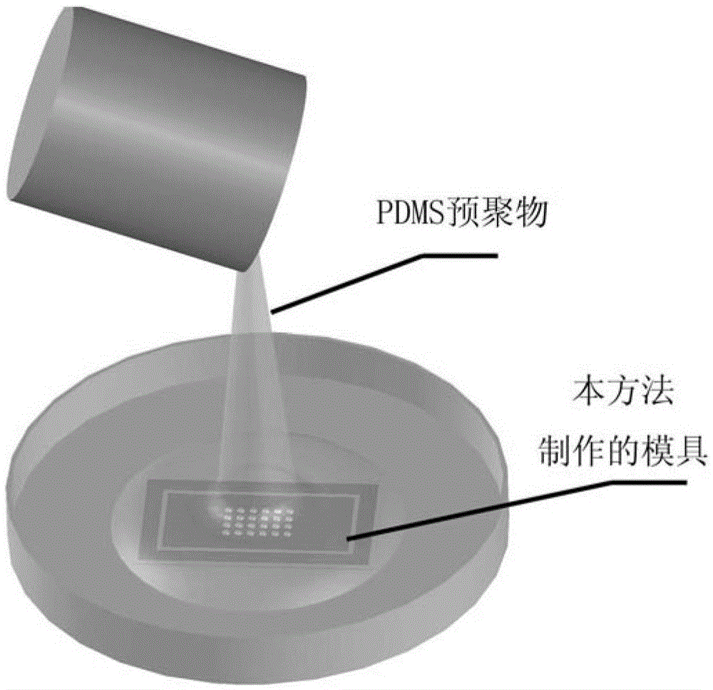
[0034] Such as image 3 As shown, the mold made is glued to the bottom of the petri dish with double-sided adhesive, poured with PDMS prepolymer, baked in an oven at 75°C for 1 hour, and then peeled off the formed PDMS to obtain PDMS with structure chip layer. Such as Figure 4 , according to the different mask patterns, you can make patterns including pipes, micro pits and their combinations. The generated pipes and dimples have curved and smooth cross-sections, such as Figure 5 shown.
PUM
 Abstract
Description
Claims
Application Information
 - R&D
- Intellectual Property
- Life Sciences
- Materials
- Tech Scout
- Unparalleled Data Quality
- Higher Quality Content
- 60% Fewer Hallucinations
Browse by: Latest US Patents, China's latest patents, Technical Efficacy Thesaurus, Application Domain, Technology Topic, Popular Technical Reports.
© 2025 PatSnap. All rights reserved.Legal|Privacy policy|Modern Slavery Act Transparency Statement|Sitemap|About US| Contact US: help@patsnap.com


